Switch device

a technology of switch and switch plate, which is applied in the direction of relays, contacts, contact mechanisms, etc., can solve the problems of short service life of contact points, difficult stabilization of contact resistance value, and inability to make second conventional microrelay smaller in size, etc., to achieve precise switching operation and higher degree of freedom of movemen

Inactive Publication Date: 2009-03-10
FUJITSU COMPONENENT LTD
View PDF16 Cites 17 Cited by
  • Summary
  • Abstract
  • Description
  • Claims
  • Application Information

AI Technical Summary

Benefits of technology

[0015]A more specific object of the present invention is to provide a switch device that can perform a more precise switching operation.
[0017]With the above structure, the movable spring is bent so that the fee end is brought into contact with the protrusion. It is thus possible to prevent portions other than the first and second contact points from being brought into contact with the movable spring and to achieve area-contact between the first and second contact points. This stabilizes the contact resistance. In addition, the movable spring with a free end has an improved degree of movement as compared to another movable spring having the two stationary contacts. Thus, a large voltage is needed to make contact with the first and second contacts.
[0022]The switch device of the present invention can perform a precise switching operation, having a higher degree of freedom in movement of the movable spring.

Problems solved by technology

Because of this, it is difficult to stabilize the value of contact resistance, and only particular spots in the contact points are abraded.
As a result, the service lives of the contact points become short.
However, the second conventional microrelay has more drawbacks than the first microrelay, in terms of the flexibility of the movable spring 510.
Therefore, the second conventional microrelay cannot be made smaller in size.

Method used


Image

  • Switch device
  • Switch device
  • Switch device

Examples


Embodiment Construction

[0063]The following is a description of switch devices as embodiments of the present invention, with reference to the accompanying drawings.

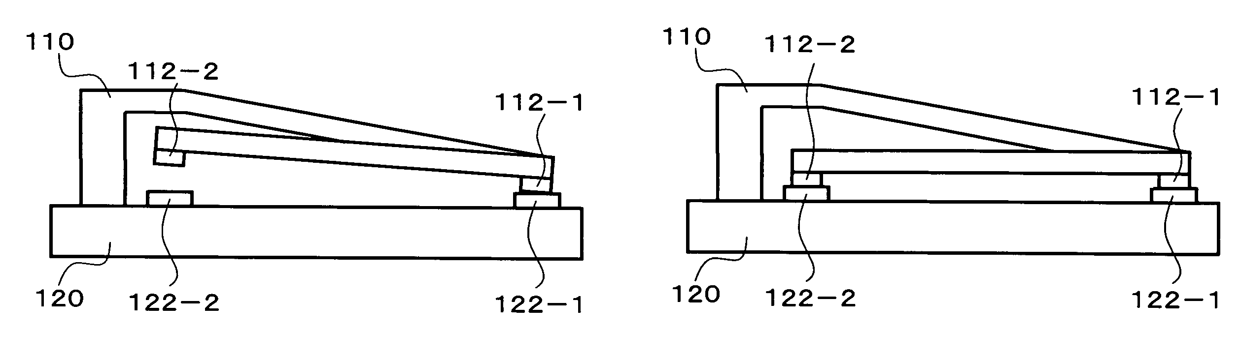
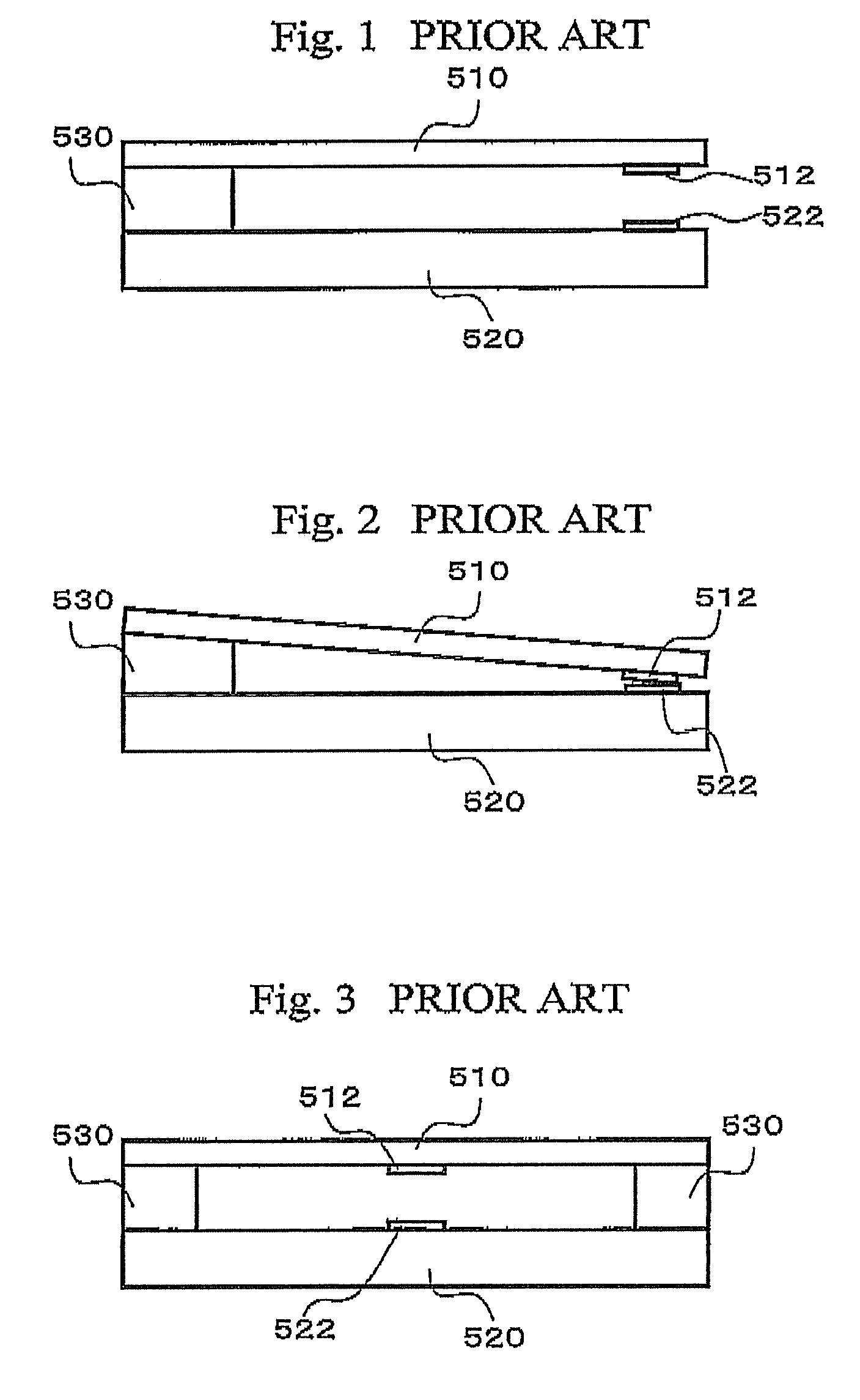
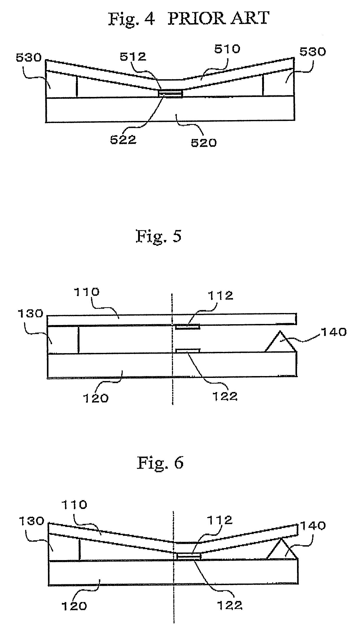
[0064]Referring first to FIG. 5, a first switch device is described. FIG. 5 is a side view of a microrelay as the first switch device. In the microrelay illustrated in FIG. 5, a movable spring 110 that is made of silicon or the like is placed above a substrate 120 that is made of silicon, Pyrex (trade name), or the like. This movable spring 110 has one end fixed by a fixing member 130 to form a fixed end, with the other end being a free end. A protrusion 140 is formed on the substrate 140. The protrusion 140 is located to vertically face the free end of the movable spring 110. The protrusion 140 is shorter than the fixing member 130. A contact point 112 that serves as a movable contact point is provided at a location slightly closer to the free end of the movable spring 110. Another contact point 122 that is a fixed contact point is provided at ...


PUM


Abstract

A switch device includes: a movable spring that has one end as a fixed end, and the other end as a free end; a substrate that is disposed below the movable spring; a first contact point that is disposed at a predetermined location between the fixed end and the free end of the movable spring; a protrusion that is formed on the substrate and is located to face the free end of the movable spring; and a second contact point that is provided on the substrate and is located to face the first contact point. This switch device is put into an ON state when the free end of the movable spring is brought into contact with the protrusion and the first contact point is brought into contact with the second contact point.

Description

BACKGROUND OF THE INVENTION[0001]1. Field of the Invention[0002]The present invention relates to a switch device that performs switching on and off of electric signals by bringing contact points into contact with each other and separating the contact points from each other.[0003]2. Description of the Related Art[0004]A microrelay that is a switch device is manufactured by semiconductor fine processing technology, and switches various electric signals such as radio-frequency signals. Such a microrelay has a number of advantageous features such as size that is smaller than a conventional relay, and therefore, has attracted public attention in recent years. Examples of such microrelays are disclosed in Japanese Unexamined Patent Publication Nos. 2001-291463, 2000-164104, 11-111146, and 2-100224, and Japanese Utility Model Gazette No. 2532487.[0005]FIG. 1 is a side view of a first conventional microrelay. In the microrelay illustrated in FIG. 1, a movable spring 510 is disposed above a ...

Claims


Application Information

Patent Timeline
Patent Type & Authority Patents(United States)
IPC IPC(8): H01H51/22
CPCH01H50/005H01H59/0009H01H2001/0063H01H2059/0054H01H2059/0072
Inventor YUBA, TAKASHIIWATA, HIDEKISEGAWA, YURIKO
Owner FUJITSU COMPONENENT LTD
Why Eureka
Try Eureka