Exposure device and image forming apparatus using the same

a technology of image forming apparatus and exposure device, which is applied in the direction of static indicating device, discharge tube luminescnet screen, instruments, etc., can solve the problems of difficult formation of interlayer insulating film, and achieve the effect of high precision and secure control

Active Publication Date: 2009-03-17
SAMSUNG DISPLAY CO LTD
View PDF24 Cites 27 Cited by
  • Summary
  • Abstract
  • Description
  • Claims
  • Application Information

AI Technical Summary

Benefits of technology

[0020]With this configuration, the intensity distribution of light emitted in the light emitting area of the EL element can be made uniform, and the channel characteristic of the light detecting element can be securely controlled. Accordingly, it is possible to detect the uniformly distributed light intensity of the EL element with high precision. Thus, it is possible to an exposure device capable of maintaining the light intensity at a constant level by controlling the light intensity of the EL element on the basis of the light detection result.

Problems solved by technology

However, it is difficult to form the interlayer insulating film 103 with a uniform thickness due to the above-described bump area resulting from the light detecting element 120.

Method used


Image

  • Exposure device and image forming apparatus using the same
  • Exposure device and image forming apparatus using the same
  • Exposure device and image forming apparatus using the same

Examples


first embodiment

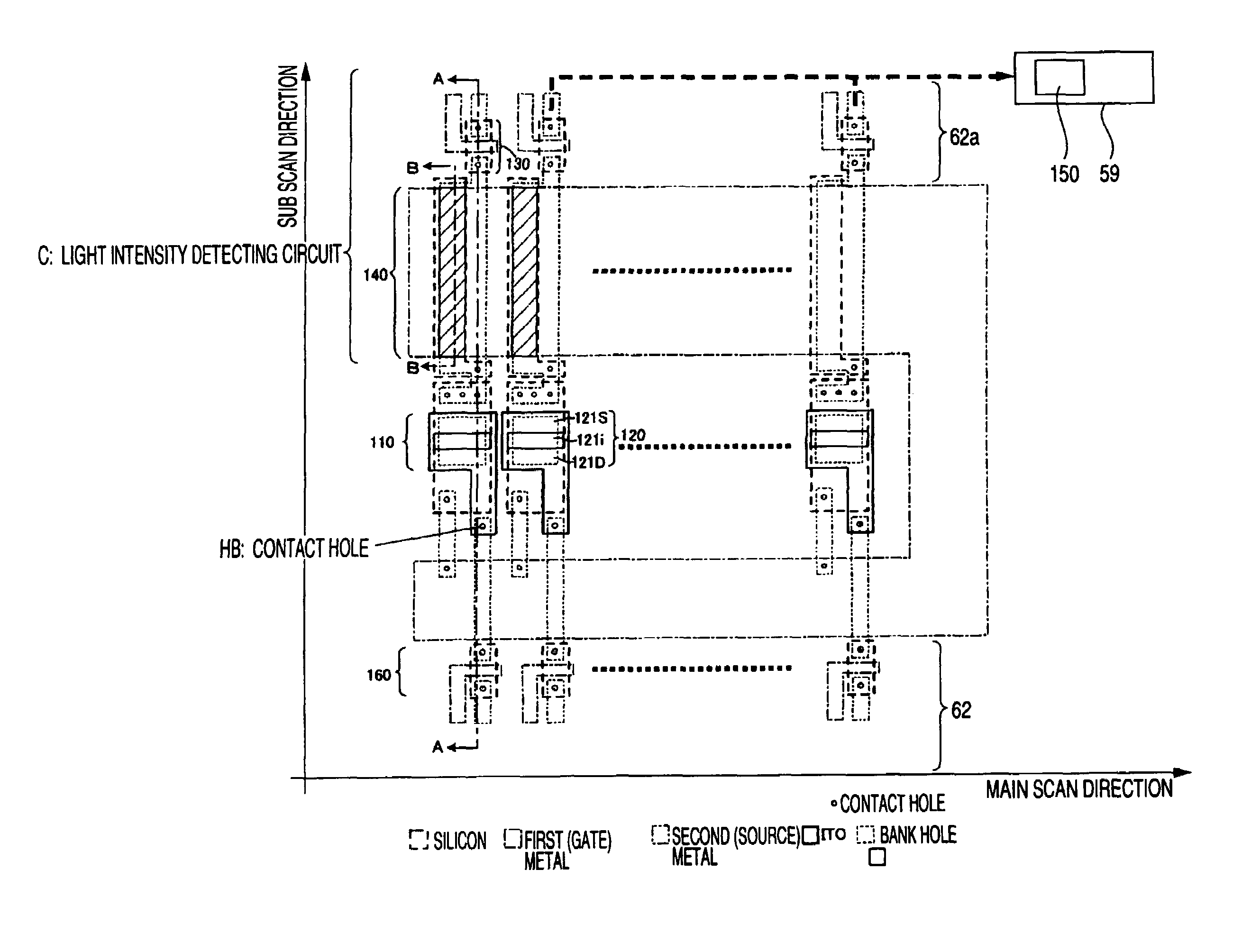
[0055]FIG. 1 is a plan view of an organic EL element constituting an exposure device and a peripheral configuration thereof in accordance with a first embodiment of the invention.

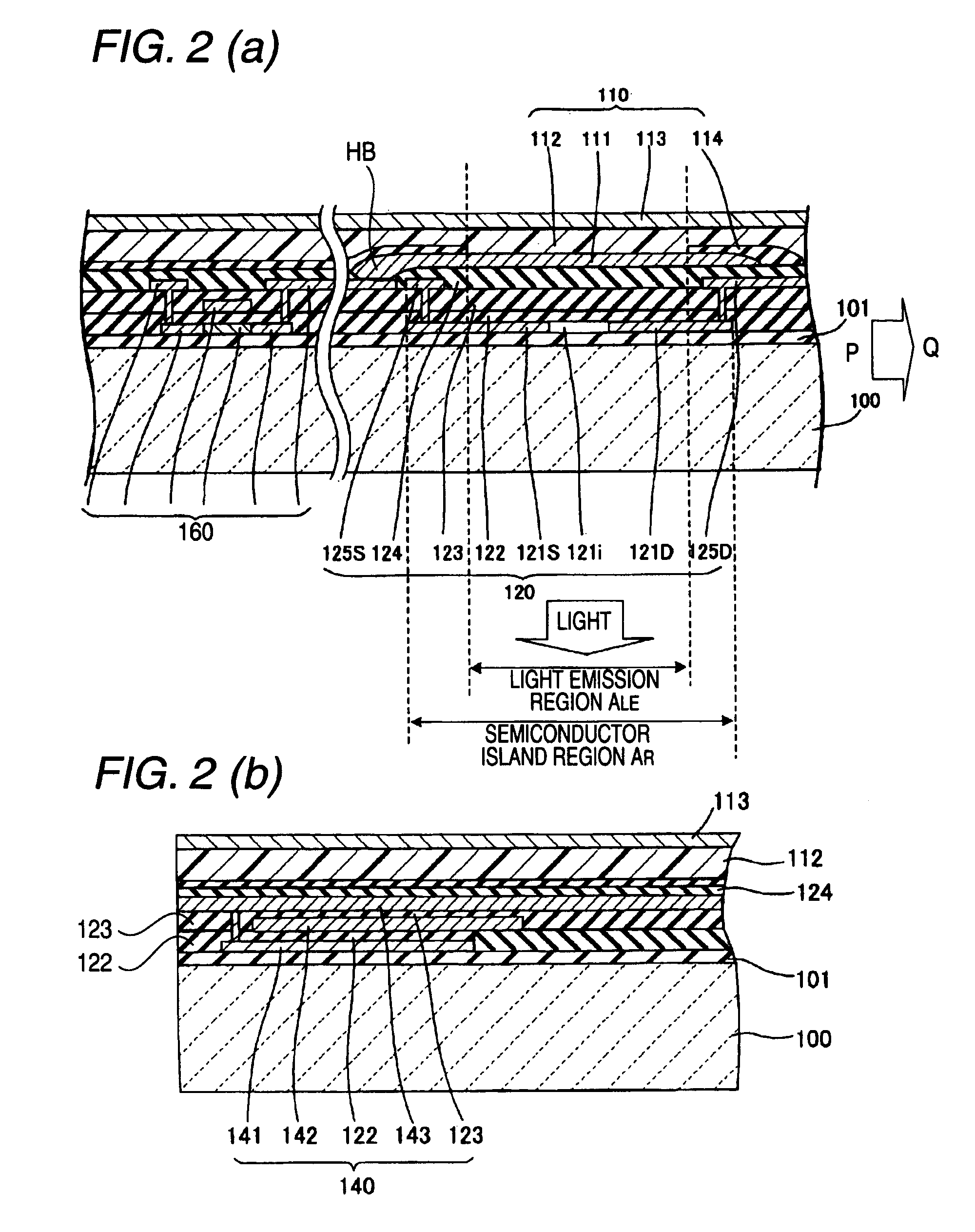
[0056]FIG. 2(a) is a cross-sectional diagram of a peripheral configuration of a light detecting element 120 in accordance with the first embodiment of the invention, FIG. 2(b) is a cross-sectional diagram showing a peripheral configuration of a capacitance element 140 in accordance with the first embodiment of the invention, and FIG. 2(c) is a cross-sectional diagram showing a peripheral configuration of a selection transistor 130 in accordance with the first embodiment of the invention.

[0057]FIG. 3 is a plan view of a main part of the organic EL element and a peripheral configuration thereof in accordance with the first embodiment of the invention.

[0058]FIGS. 2(a) and 2(c) are taken along the line A-A in FIG. 1, and FIG. 2(b) is taken along the line B-B in FIG. 1. The portion Q in FIG. 2(c) is continuous w...

second embodiment

[0223]Next, an image forming apparatus using the exposure device described in connection with the first embodiment will be described as a second embodiment.

[0224]FIG. 18 is a diagram showing a configuration of an image forming apparatus in accordance with a second embodiment of the invention.

[0225]FIG. 18 shows an image forming apparatus 1 having, as the exposure device, exposure devices 13Y to 13K corresponding to each color of yellow, magenta, cyan, and black.

[0226]As shown in FIG. 18, the image forming apparatus 1 includes four development stations corresponding to four colors, i.e., a yellow development station 2Y, a magenta development station 2M, a cyan development station 2C, and a black development station 2K, which are arranged with an offset in a longitudinal direction. A paper feeding tray 4 accommodating a recording paper 3 as a recording medium therein is disposed above the development stations 2Y to 2K. At locations corresponding to the individual development stations ...

third embodiment

[0372]FIGS. 27(a) and 27(b) are explanatory diagrams showing examples of an element arrangement pattern in the exposure device in accordance with a third embodiment of the invention.

[0373]Next, a modified example of the element arrangement pattern in accordance with the third embodiment of the invention will be described.

[0374]Although in the first embodiment, as shown by a schematic diagram in FIG. 27(a), the selection transistor 130, the capacitance element 140, and the light detecting element 120 are aligned in a line shape in a direction substantially vertical to the light emitting element array (see FIG. 1 for reference), the capacitance element 140 may be shifted from the line arrangement of the selection transistor 130 and the light detecting element 120 in a zigzag configuration, as shown by a schematic diagram in FIG. 27(b). In FIG. 27, reference numeral 110 denotes the organic EL element.

[0375]Although in the above-described embodiments, an example of the light detecting e...


PUM


Abstract

To provide an exposure device and an image forming apparatus using the same, in which the exposure device can detect light intensity with improved reliability and thereby controls the light intensity with high precision, the exposure device includes an EL (electro-luminescence) element having a first electrode (an anode), a second electrode (a cathode), and a light emitting layer disposed between the first and second electrodes, thereby forming a light emitting unit, and a light detecting element detecting light emitted from the EL element, in which the EL element and the light detecting element are stacked onto each other. The light detecting element is provided at an inner side of a principal surface of the electrode (the anode) which is disposed closer to the light detecting element than the other electrode. A light emitting area of the EL element is provided at an inner side of a principal surface of the light detecting element.

Description

BACKGROUND OF THE INVENTION[0001]1. Field of the Invention[0002]The present invention relates to an exposure device and an image forming apparatus using the same, and more particularly, to an exposure device and an image forming apparatus using the exposure device in which light emitting elements are aligned in an array configuration.[0003]2. Description of the Related Art[0004]With the recent trend toward a smaller and cheaper image forming apparatus such as a facsimile machine or a printer, there have been many attempts to make smaller and cheaper components of the image forming apparatus.[0005]In an image forming apparatus employing an electro-photographic process, a photosensitive member is exposed to light by irradiating light modulated with image data onto the photosensitive member, and a toner adhering to the photosensitive member by the electrostatic force is transferred onto a printing medium such as a recording paper, thereby forming an image on the printing medium. As a m...

Claims


Application Information

Patent Timeline
Patent Type & Authority Patents(United States)
IPC IPC(8): H01L27/15H04N1/031
CPCB41J2/45H01L27/3269H10K59/13
Inventor NAKAMURA, TETSUROUSHIROUZU, HIROSHIHAMANO, TAKAFUMIYAMAMOTO, SHINYA
Owner SAMSUNG DISPLAY CO LTD
Why Eureka
Try Eureka