Radioactive ray detector

a radiation detector and detector technology, applied in the field of radiation detectors, can solve problems such as degradation in the characteristics of radiation detectors such as sensitivity, reliability, life, etc., and achieve the effect of suppressing radiation transmitting the wiring substra

Inactive Publication Date: 2009-03-24
HAMAMATSU PHOTONICS KK
View PDF15 Cites 35 Cited by
  • Summary
  • Abstract
  • Description
  • Claims
  • Application Information

AI Technical Summary

Benefits of technology

[0008]According to such an arrangement, a portion with no through hole in the wiring substrate allows the glass material thereof to suppress radiation transmitting from the signal input surface to the signal output surface. Even another portion with a through hole in the wiring substrate will also allow radiation having passed through the through hole not to be made incident on the signal processing means. This realizes a radiation detector which suppresses radiation made incident on the signal processing means irrespective of the presence of the through hole in the wiring substrate.
[0012]According to such an arrangement, a portion with no through hole in the wiring substrate allows the glass material thereof to suppress radiation transmitting from the signal input surface to the signal output surface. Another portion with a through hole in the wiring substrate will also allow the shield member to suppress radiation passing through the through hole. This arrangement realizes a radiation detector which suppresses radiation made incident on the signal processing means irrespective of the presence of the through hole in the wiring substrate.
[0013]In the above-mentioned arrangement, the shield member is preferably configured such that a predetermined shield material having a radiation shielding function is filled in the through hole. Alternatively, the shield member is preferably a bump electrode which is formed of a predetermined shield material having a radiation shielding function and which is electrically connected to the conductive member provided in the through hole. These arrangements make it possible to shield against radiation in a simple manner in the through hole of the wiring substrate. It is also acceptable to employ other arrangements.
[0014]As for the glass material used for the wiring substrate, the glass substrate is preferably formed of a glass material that contains lead. This allows for effectively suppressing radiation transmitting the wiring substrate. It is also acceptable to employ a substrate formed of another glass material having a radiation shielding function.

Problems solved by technology

In this case, the scintillator, the photodetecting element array, the wiring substrate, and the signal processing element may be located along a predetermined alignment direction, and this arrangement raises a problem that the radiation having transmitted the scintillator and the like transmits the wiring substrate to be made incident upon the signal processing element located downstream of the arrangement.
The radiation made incident on the signal processing element in this manner would result in damage to the signal processing element due to the radiation, thereby causing degradation in the characteristics of the radiation detector such as sensitivity, reliability, or life.

Method used


Image

  • Radioactive ray detector
  • Radioactive ray detector
  • Radioactive ray detector

Examples


first embodiment

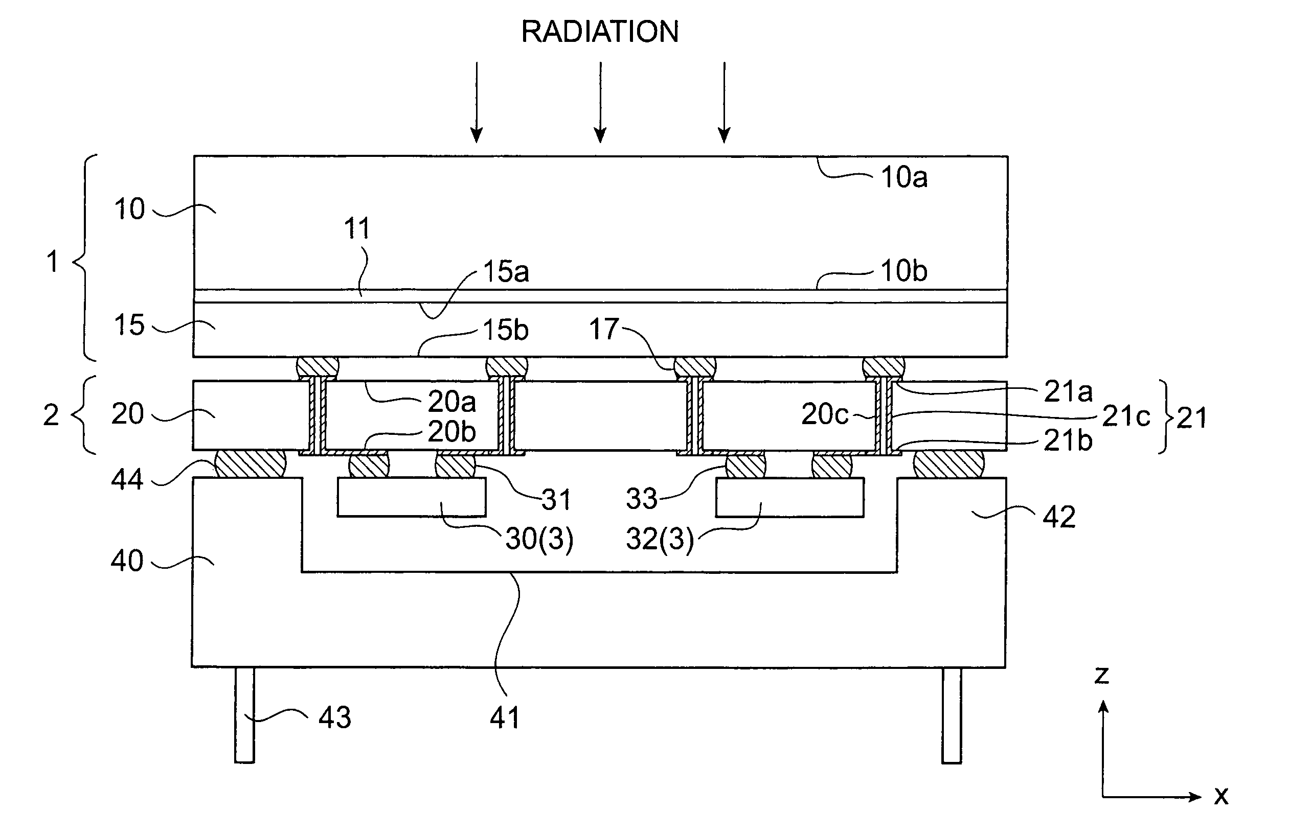
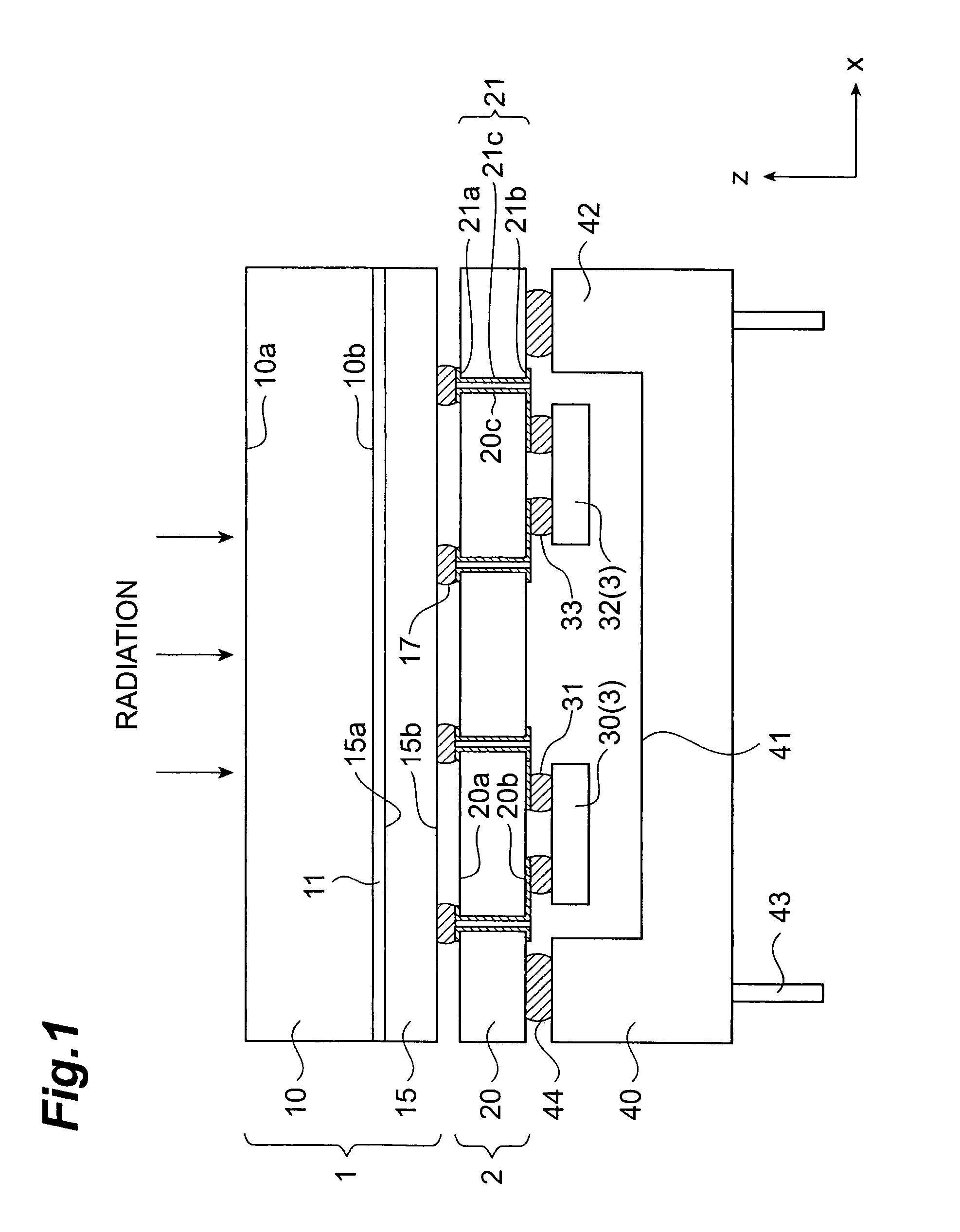
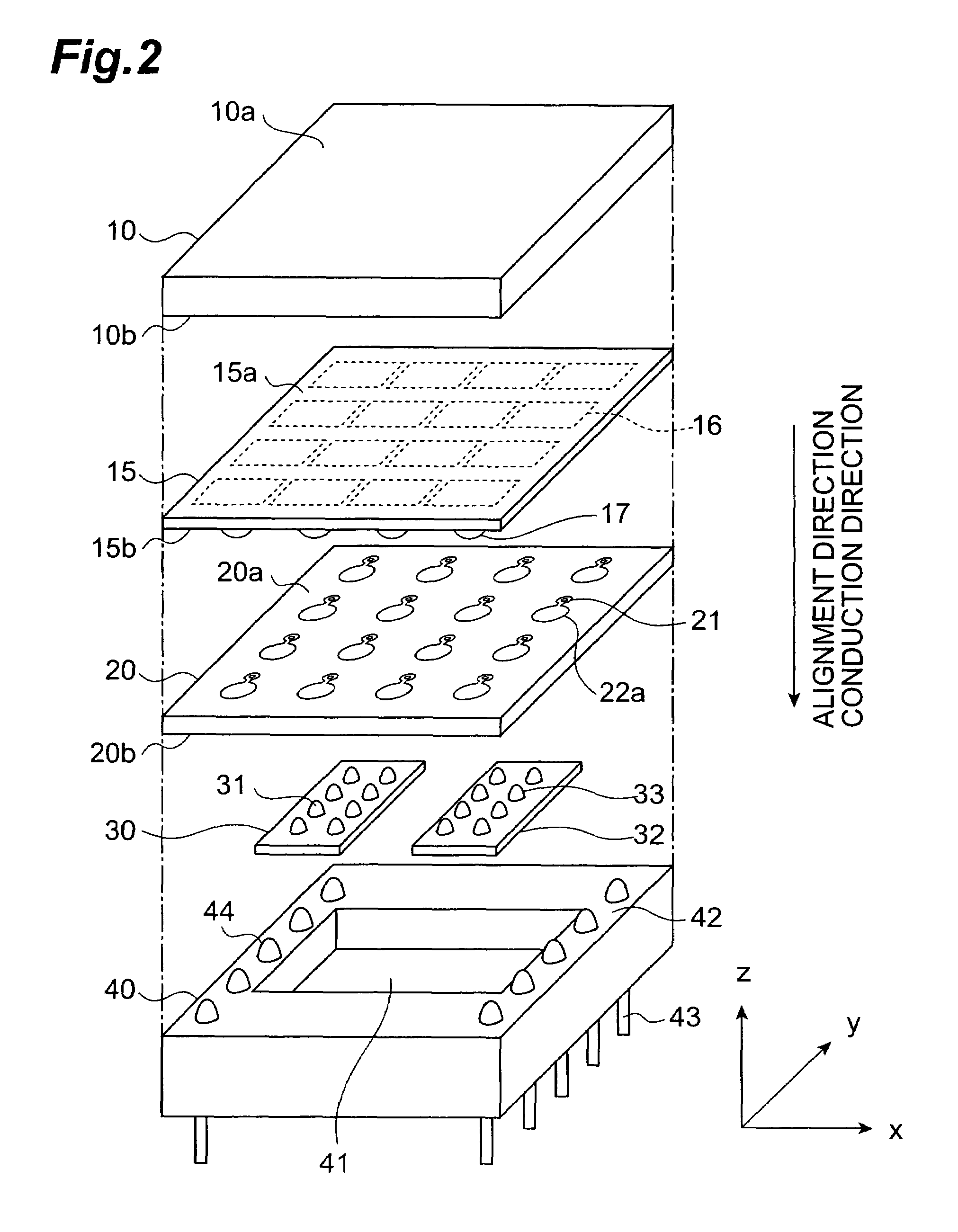
[0034]FIG. 1 is a sectional side view illustrating the sectional structure of a radiation detector according to the present invention. FIG. 2 is an exploded perspective view illustrating components in the configuration of the radiation detector shown in FIG. 1. For convenience in description, as shown in FIG. 1 and FIG. 2, it is defined in each of the following drawings that radiation is incident along the direction of z-axis, and two axes orthogonal to the z-axis are the x-axis and y-axis. In the configuration herein, the negative direction of the z-axis is the conduction direction from a signal input surface to a signal output surface in the wiring substrate, and the alignment direction of the components in the radiation detector.

[0035]The radiation detector shown in FIG. 1 includes a radiation detecting section 1, a wiring substrate section 2, and a signal processing section 3. As shown in FIG. 2, these components are arranged in that order from the upstream side (the upper side ...

second embodiment

[0081]FIG. 7 is a sectional side view illustrating the sectional structure of a radiation detector according to a FIG. 8 is an exploded perspective view illustrating components in the configuration of the radiation detector shown in FIG. 7.

[0082]The radiation detector shown in FIG. 7 includes the radiation detecting section 1, the wiring substrate section 2, the signal processing section 3, and the housing 40. Of these components, the configurations of the radiation detecting section 1 and the housing 40 are the same as those of the embodiment shown in FIG. 1.

[0083]The wiring substrate section 2 is located downstream of the radiation detecting section 1. In this embodiment, the wiring substrate section 2 has a wiring substrate 25 in which provided is a conduction path for guiding an electric signal between the signal input surface and the signal output surface. The wiring substrate 25 employs, as its substrate, a glass substrate formed of a predetermined glass material having a rad...

third embodiment

[0114]FIG. 13 is a sectional side view illustrating the sectional structure of a radiation detector according to a FIG. 14 is an exploded perspective view illustrating components in the configuration of the radiation detector shown in FIG. 13. In FIG. 14, the scintillator 10 and the housing 40 are not illustrated.

[0115]The radiation detector shown in FIG. 13 includes the radiation detecting section 1, a wiring substrate section 6, the signal processing section 3, and the housing 40. Of these components, the configurations of the radiation detecting section 1 and the housing 40 are the same as those of the embodiment shown in FIG. 1.

[0116]The wiring substrate section 6 is located downstream of the radiation detecting section 1. In this embodiment, the wiring substrate section 6 has a wiring substrate 60 in which provided is a conduction path for guiding an electric signal between the signal input surface and the signal output surface. The wiring substrate 60 employs, as its substrat...


PUM


Abstract

A wiring substrate section 2 is provided between a radiation detecting section 1, which is formed of a scintillator 10 and a PD array 15, and signal processing elements 30 and 32 for processing a detected signal outputted from the PD array 15, and the wiring substrate section 2 has a wiring substrate 20 which is formed of a glass material having a radiation shielding function and in which a conductive member 21 serving as a conduction path for guiding the detected signal therethrough is provided in a through hole 20c. Relative to the through hole 20c of the wiring substrate 20, the signal processing elements 30 and 32 of the signal processing section 3, located downstream of the wiring substrate 20, are each disposed in an area excluding those areas on the extension of the through holes 20c, and this allows the signal processing elements 30 and 32 not to be seen through the through holes 20c. This arrangement realizes a radiation detector which suppresses radiation made incident on the signal processing means located downstream of the wiring substrate.

Description

TECHNICAL FIELD[0001]This invention relates to a radiation detector in which employed is a wiring substrate with a conduction path for guiding an electric signal.BACKGROUND ART[0002]Radiation detectors for use with CT sensors include a detector with a scintillator placed on the light-incident surface of a semiconductor photodetecting element array such as a photodiode array. In such a radiation detector, when the radiation to be detected is made incident on the scintillator, such as X-rays, gamma rays, or charged particles, scintillation light is generated by the radiation in the scintillator. The scintillation light is then detected with the semiconductor photodetecting elements, thereby allowing the radiation to be detected.[0003]The photodetecting element array is also provided with a signal processing element for processing a detected signal that is outputted from each photodetecting element. In this case, the photodetecting element and the signal processing element can be elect...

Claims


Application Information

Patent Timeline
Patent Type & Authority Patents(United States)
IPC IPC(8): G01T1/26G01T1/20G01T1/24H01L27/14H01L27/146H01L31/0232H01L31/09H04N5/32
CPCG01T1/2018H01L31/02322H01L27/14661H01L27/14634G01T1/2019G01T1/20185G01T1/24G01T1/20187
Inventor SHIBAYAMA, KATSUMIKUSUYAMA, YUTAKAHAYASHI, MASAHIRO
Owner HAMAMATSU PHOTONICS KK
Why Eureka
Try Eureka