Printed wiring board including power supply layer and ground layer

a technology of printed wiring and ground layer, which is applied in the incorporation of printed electric components, cross-talk/noise/interference reduction, printed circuit aspects, etc., can solve the problem that the noise of power supply is forced to inevitably pass through the electrically-conductive pieces, and the electric current is forced to be qui

Active Publication Date: 2007-06-28
FUJITSU LTD
View PDF4 Cites 20 Cited by
  • Summary
  • Abstract
  • Description
  • Claims
  • Application Information

AI Technical Summary

Benefits of technology

[0015] Otherwise, the printed wiring board may further comprise: a third insulating layer; a third electrically-conductive ground layer formed on the surface of the third insulating layer; an island of a fourth electrically-conductive ground layer contoured based on a projected image of the electronic circuit element, the fourth electrically-conductive ground layer isolated from the third electrically-conductive ground layer on the surface of the third insulating layer; a third electrically-conductive piece connecting the fourth electrically-conductive ground layer to the third electrically-conductive ground layer; and vias connecting the second and fourth electrically-conductive ground layers to each other at positions outside the second electrically-conductive power supply layer located in a space between the second and fourth electrically-conductive ground layers. The vias function as a shield for the island of the second electrically-conductive power supply layer. This results in a significant reduction of radiation of electromagnetic waves from the second electrically-conductive power supply layer.

Problems solved by technology

Noise in the electric current, namely power supply noise is forced to inevitably pass through the electrically-conductive pieces.

Method used


Image

  • Printed wiring board including power supply layer and ground layer
  • Printed wiring board including power supply layer and ground layer
  • Printed wiring board including power supply layer and ground layer

Examples


Embodiment Construction

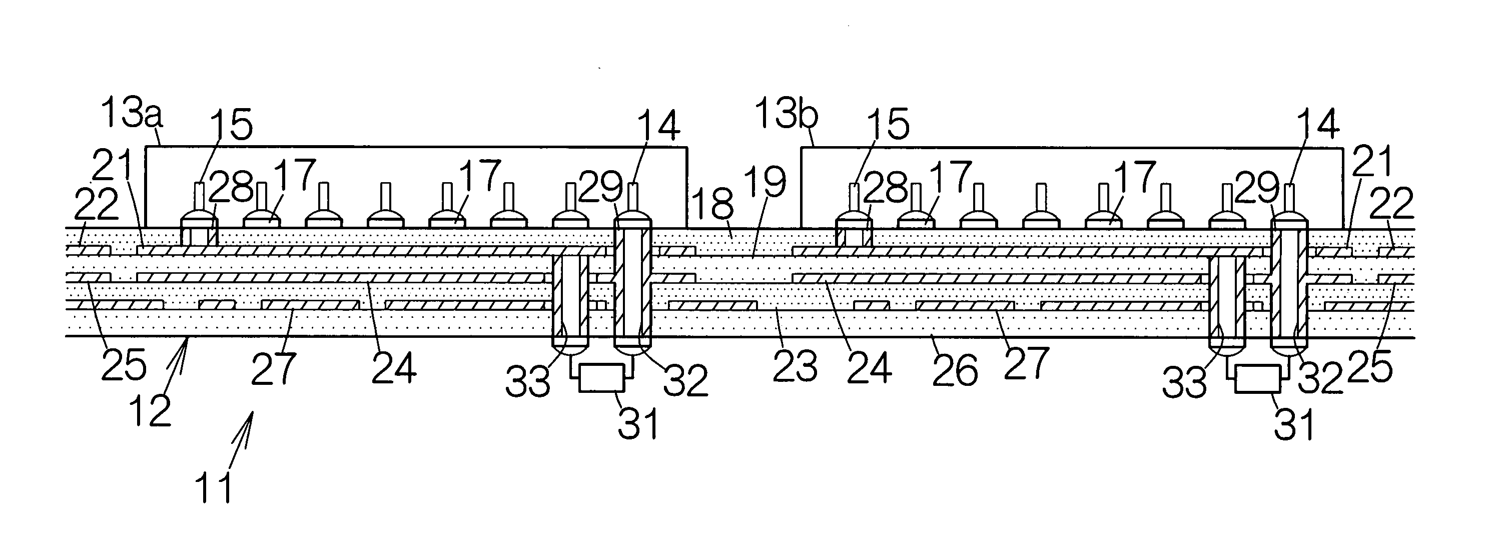
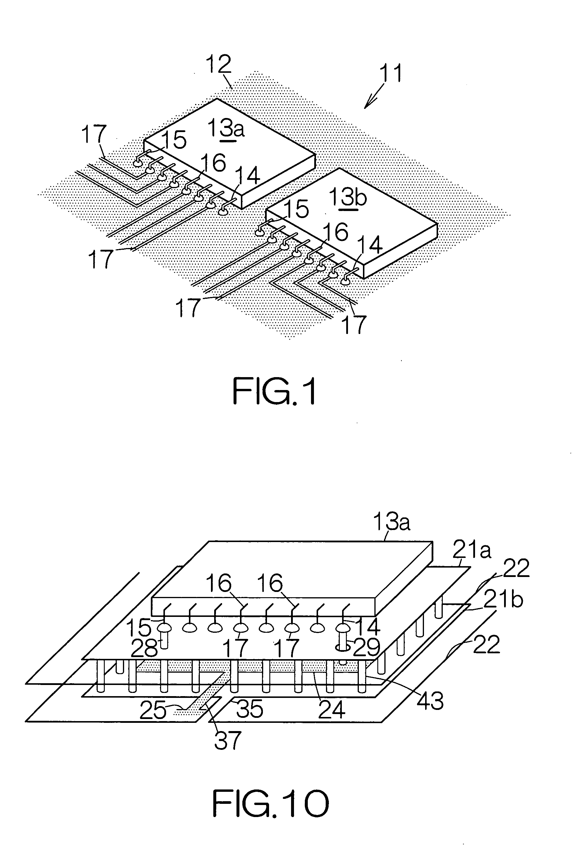
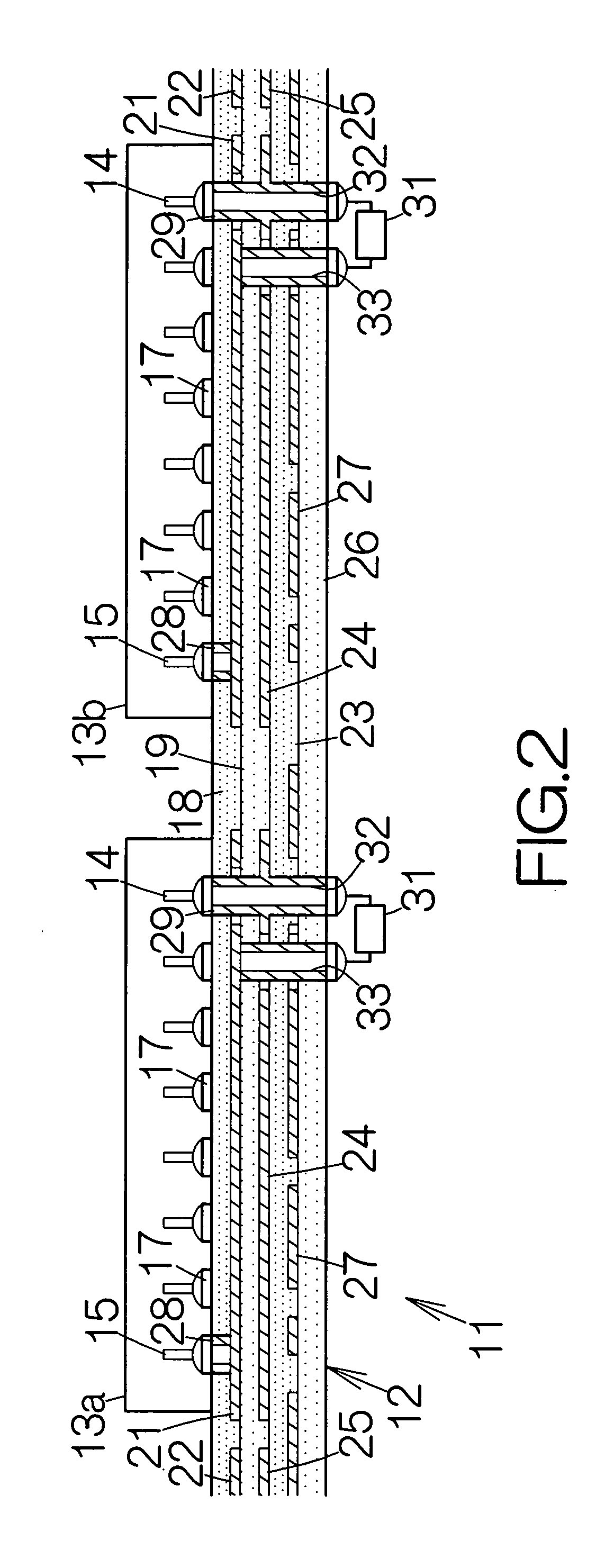
[0027]FIG. 1 schematically illustrates a printed circuit board unit 11 according to an embodiment of the present invention. The printed circuit board unit 11 includes a printed wiring board 12. One or more LSI (Large-Scale Integrated circuit) chip or chips 13a, 13b, . . . are mounted on the front surface of the printed wiring board 12, for example. A power supply pin 14, a ground pin 15 and signal pins 16 are connected to each of the LSI chips 13a, 13b.

[0028] Wiring patterns 17 are formed on the surface of the printed wiring board 12. The wiring patterns 17 may be made of an electrically-conductive material such as copper, for example. The signal pins 16 are soldered to the corresponding wiring patterns 17, respectively.

[0029] As shown in FIG. 2, the wiring patterns 17 are received on the uppermost layer of the printed wiring board 12, namely the upper surface of a first insulating layer 18. The first insulating layer 18 is received on the upper surface of a second insulating laye...


PUM


Abstract

A first power supply layer spreads over an insulating layer outside an island of a second power supply layer. A first ground layer spreads over an insulating layer outside an island of a second ground layer. First and second electrically-conductive pieces are interposed between the first and second power supply layers as well as between the first and second ground layers. A capacitor is interposed between the first and second electrically-conductive pieces. Power supply noise is forced to inevitably pass through the electrically-conductive pieces. The power supply noise thus reliably flows into the capacitor through the first and second electrically-conductive pieces. A printed wiring board is in this manner allowed to enjoy a sufficient suppression of the power supply noise.

Description

BACKGROUND OF THE INVENTION [0001] 1. Field of the Invention [0002] The present invention relates to a printed wiring board including an electrically-conductive power supply layer and an electrically-conductive ground layer. [0003] 2. Description of the Prior Art [0004] A printed wiring board usually includes an electrically-conductive power supply layer and an electrically-conductive ground layer. A LSI (Large-Scale Integrated circuit) chip is mounted on the surface of the printed wiring board. The LSI chip is connected to the electrically-conductive power supply layer and the electrically-conductive ground layer. A chip capacitor, namely a bypass capacitor, is connected to the electrically-conductive power supply layer and the electrically-conductive ground layer. The bypass capacitor serves to reduce power supply noise. [0005] Japanese Patent Application Publication Nos. 6-244562 and 11-233951 disclose an island of an electrically-conductive power supply layer and an island of an...

Claims


Application Information

Patent Timeline
Patent Type & Authority Applications(United States)
IPC IPC(8): H05K1/16
CPCH05K1/0225H05K1/0231H05K1/0298H05K2201/093H05K2201/09309H05K2201/09663H05K2201/10545H05K2201/10689
Inventor NAKAO, TOMOYUKI
Owner FUJITSU LTD
Why Eureka
Try Eureka