Semiconductor device with bypass capacitor

Inactive Publication Date: 2005-01-20
YAMAHA CORP
View PDF9 Cites 20 Cited by
  • Summary
  • Abstract
  • Description
  • Claims
  • Application Information

AI Technical Summary

Benefits of technology

[0014] Since a laminated electrode capacitance and a MOS capacitance can be utilized, a large capacitance can be formed between the power source vol

Problems solved by technology

However, it is difficult to perfectly prevent a power source voltage fluctuation inside IC and malfunctions and noises of the IC internal circuits by the external electrostatic discharge etc.
Power source noises generated by the operation of internal circuits of IC are hard to be sufficiently absorbed by the bypass capacitor.
Power source noises generated inside IC leak to the external from signal input/output pads so that IC becomes a high frequency noise source.
Power source noises generated inside IC i

Method used


Image

  • Semiconductor device with bypass capacitor
  • Semiconductor device with bypass capacitor
  • Semiconductor device with bypass capacitor

Examples


Embodiment Construction

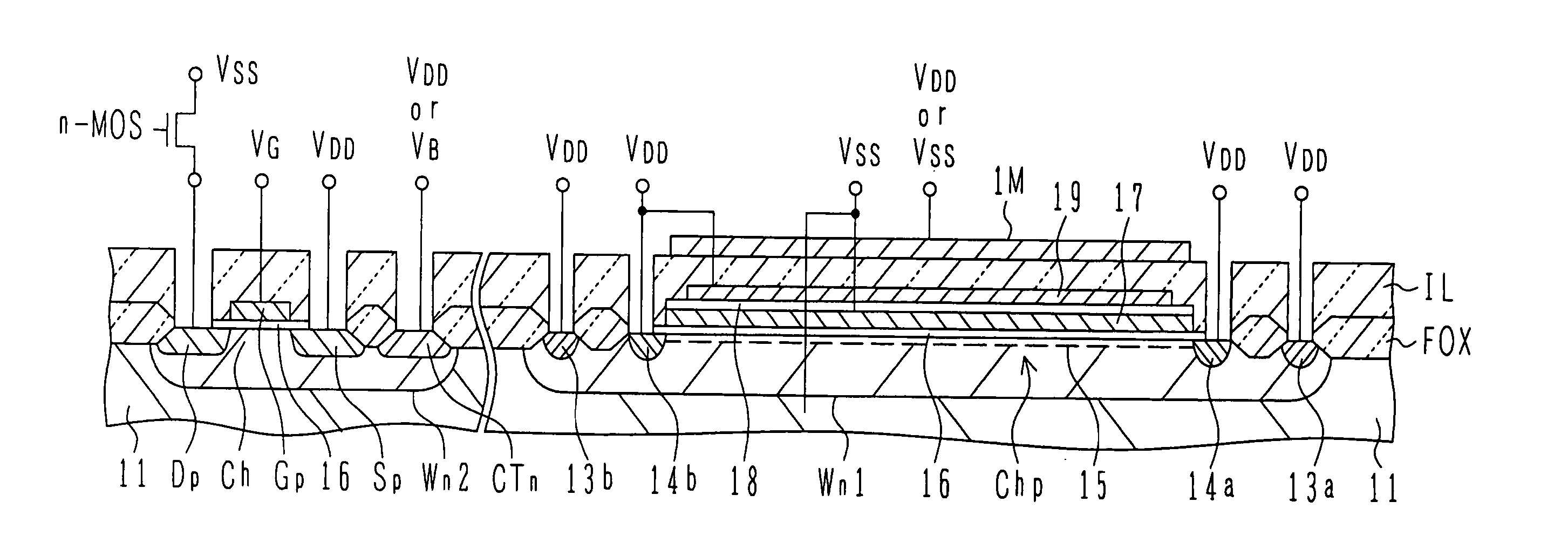
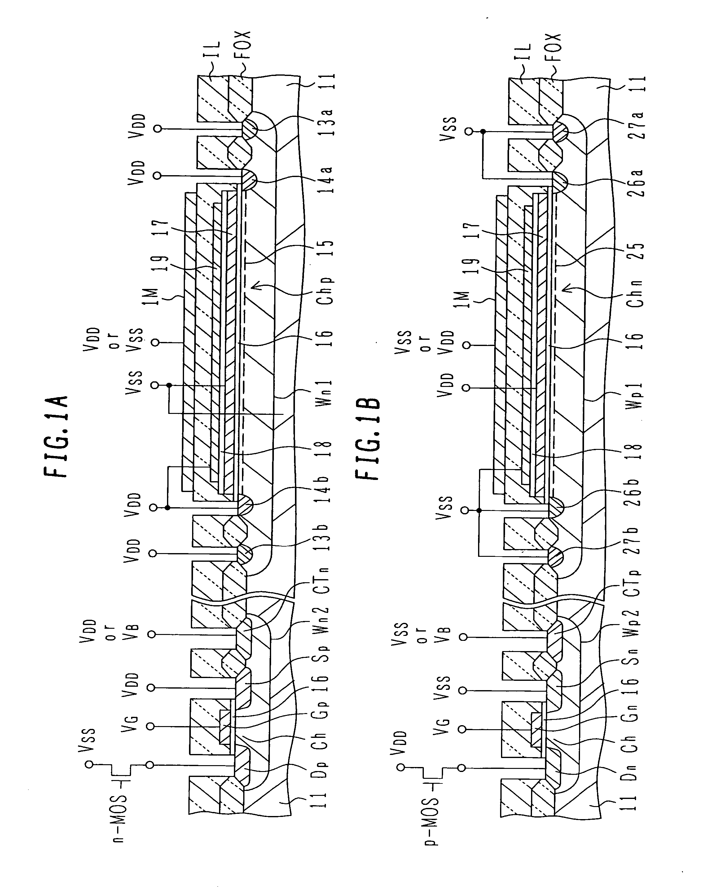
[0024] In the following, description will be made on a semiconductor device having a bypass capacitor according to an embodiment of the invention, with reference to the accompanying drawings. Although a semiconductor device having an n-type active region and a semiconductor device having a p-type active region will be described, these devices may be integrated to form a complementary (C) MOS integrated circuit. In the description, a power source voltage VDD is a positive voltage and VSS is a ground voltage.

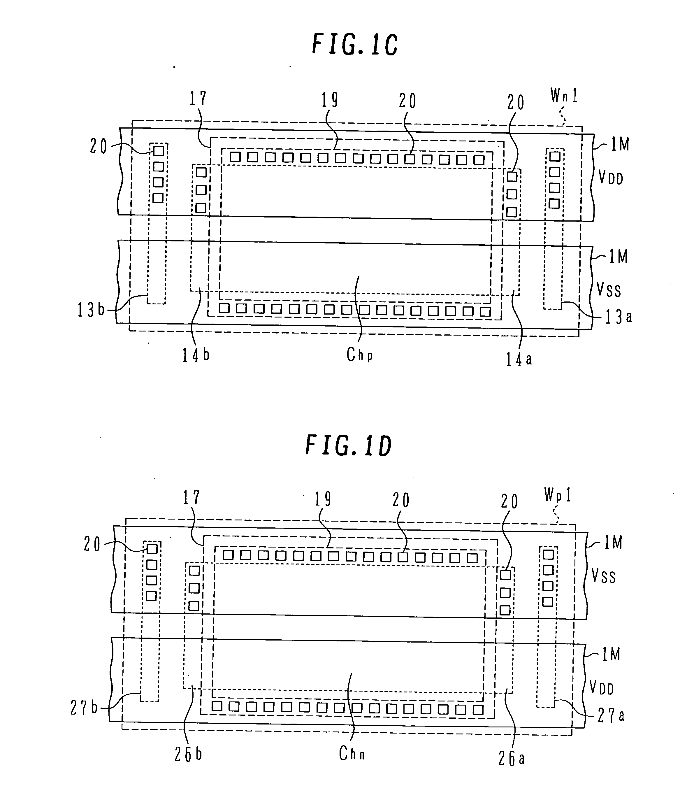
[0025] As shown in FIG. 1A, on the surface of a p-type silicon substrate 11, a field oxide film FOX is formed to define active regions. In FIG. 1A, although the field oxide film is formed by local oxidation of silicon (LOCOS), it may be formed by shallow trench isolation (STI). Impurity ions of an n-type are implanted into active regions to form a first n-type well Wn1 for a bypass capacitor and a second n-type well Wn2 for a p-channel MOS transistor.

[0026] The surface of the ac...


PUM


Abstract

A semiconductor device comprises a semiconductor substrate having first and second active regions of first conductivity type, first and second insulated electrodes crossing the first and second active regions, respectively, a third insulated electrode formed on the second insulated electrode, source/drain regions formed on both sides of the first electrode, pseudo source/drain regions formed on both sides of the second electrode, first and second power source lines formed above the second active region through an interlevel insulating layer, a first interconnection connecting the third electrode and the pseudo source/drain regions to the first power source line, and a second interconnection connecting the second electrode to the second power source line, wherein the first active region constitutes a MOS transistor and the second active region constitutes a bypass capacitor and induces an inversion layer of the second conductivity type under the second electrode structure when the power source lines are activated.

Description

CROSS REFERENCE TO RELATED APPLICATION [0001] This application is based on and claims priority of Japanese Patent Application No. 2003-199277 filed on Jul. 18, 2003, the entire contents of which are incorporated herein by reference. BACKGROUND OF THE INVENTION [0002] A) Field of the Invention [0003] The present invention relates to a semiconductor integrated circuit (IC) device to be used with a portable equipment and the like, and more particularly to a semiconductor device aiming at suppressing a power source voltage fluctuation and unnecessary radiation. [0004] B) Description of the Related Art [0005] As shown in FIG. 4A, when a semiconductor integrated circuit (IC) package 110 is mounted on a printed circuit board 120 or the like and used with other circuits, a bypass capacitor 103 of about 1 μF is externally connected between a lead 101 for a package power source voltage and a ground plane 102 of the printed circuit board to suppress a fluctuation of the voltage to be supplied ...

Claims


Application Information

Patent Timeline
IPC IPC(8): H01L21/02H01L21/334H01L27/06H01L27/108H01L29/00H01L29/76
CPCH01L27/0629H01L29/66181H01L28/40
Inventor SEKIMOTO, YASUHIKO
Owner YAMAHA CORP
Why Eureka
Try Eureka