AI technical title is built by Patsnap AI team. It summarizes the technical point description of the patent document.
a field effect transistor and transistor technology, applied in the field of field effect transistors, can solve the problems of scaling having its limits, and achieve the effect of selectively increasing the effective channel length (leff) and the transistor siz
Inactive Publication Date: 2009-03-31
INT BUSINESS MASCH CORP
View PDF7 Cites 3 Cited by
Summary
Abstract
Description
Claims
Application Information
AI Technical Summary
This helps you quickly interpret patents by identifying the three key elements:
Problems solved by technology
Method used
Benefits of technology
Benefits of technology
[0005]In view of the foregoing, disclosed above are embodiments of a field effect transistor (FET) that incorporates a semiconductor body with a spiral-shaped center channel region wrapped one or more times around a gate and with end regions that extend outward from the center region in opposite directions away from the gate. Source / drain regions are formed in the end regions by either doping the end regions or by biasing a back gate to impart a preselected Fermi potential on the end regions. This disclosed structure allows the transistor size to be scaled without decreasing the effective channel length (Leff) to the point where deleterious short-channel effects are exhibited. It further allows the transistor size to be scaled while also allowing the effective channel length (Leff) to be selectively increased (e.g., by increasing the number of times the channel wraps around the gate). Also, disclosed are embodiments of an associated method of forming the transistor.
Problems solved by technology
However, recently it has been determined that such scaling has its limits because short channel lengths can lead to undesirable “short-channel effects” including, but not limited, variability in threshold voltage and excessive drain leakage currents.
Method used
Image
Click on the blue label to locate the original text in one second.
Reading with bidirectional positioning of images and text.
Examples
embodiment 100
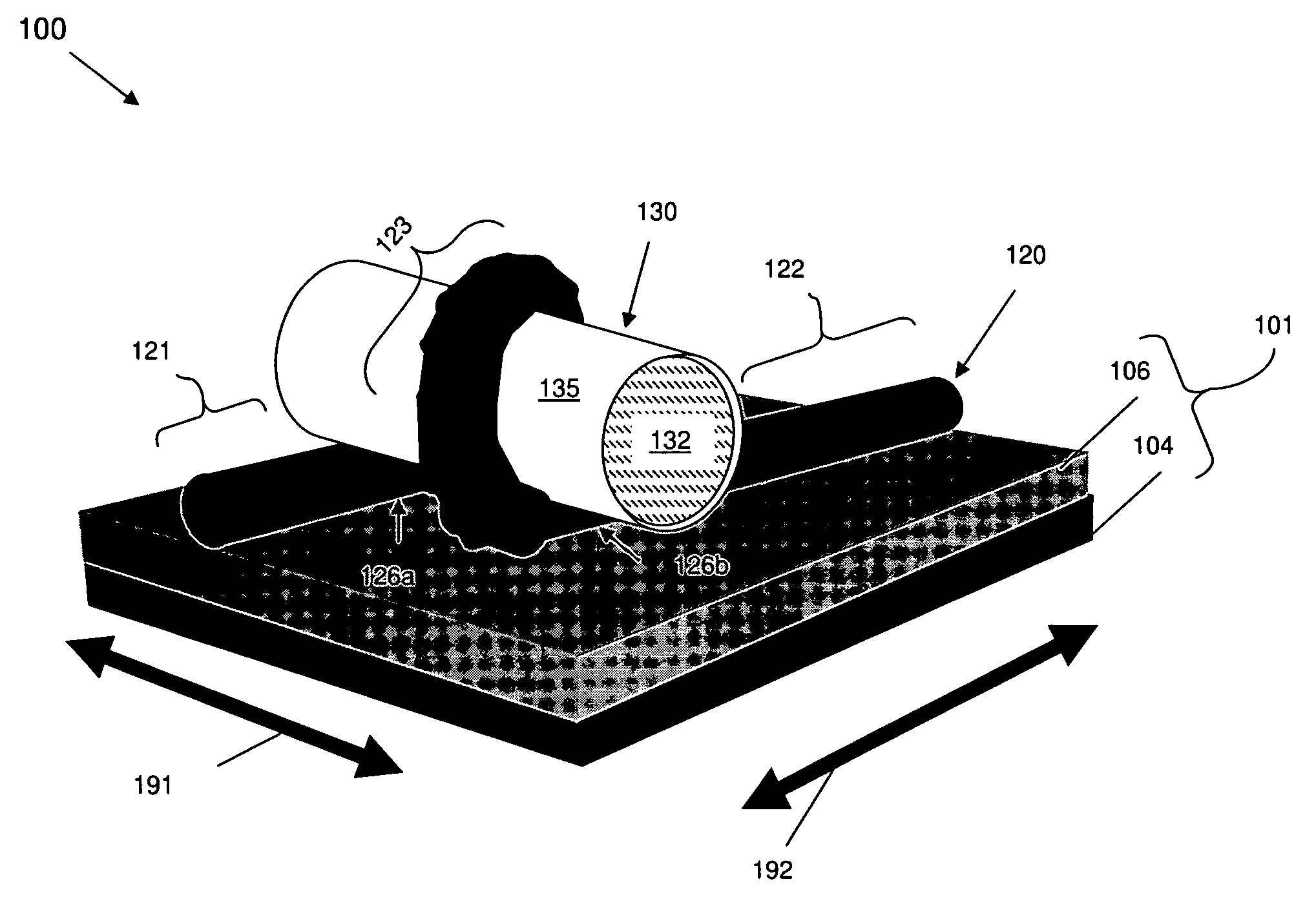
[0074]More particularly, referring to FIG. 8, a transistor embodiment 100 of FIG. 1 with a carbon nanotube semiconductor body 120 can be formed, for example, by providing a multi-layer substrate (802). For example, a substrate 101a can be provided that comprises an isolation layer 106a (e.g., an oxide layer or other dielectric layer) on a conductor layer 104a (e.g., a doped semiconductor layer, such as a doped silicon or polysilicon layer, or a metal layer) (see FIG. 9a). Alternatively, a substrate 101b can be provided that comprises isolation layer 106b (e.g., a quartz layer or an oxide layer) on a semiconductor layer 104b (e.g., on a silicon layer) (see FIG. 9b). Then, a carbon nanotube 120 can be formed (e.g., deposited) on the substrate 101a, 101b (804, see FIGS. 9a and 9b).
[0075]This carbon nanotube 120 can be formed using conventional carbon nanotube processing techniques, for example, arc evaporation, or passing of carbon-containing gases over nanoparticles of Co, Fe, or Ni, ...
embodiment 200
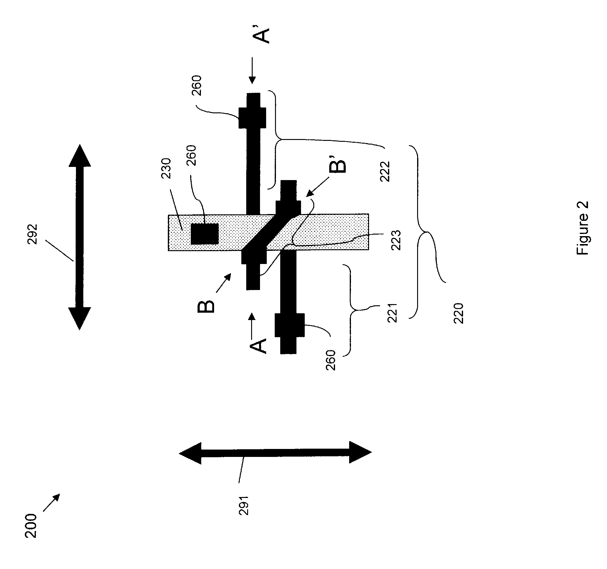
[0079]Alternatively, referring to FIG. 21, the transistor embodiment 200 of FIGS. 2-4 with a polysilicon or silicon semiconductor body 220 can be formed, for example, by first providing a wafer comprising a multi-layer substrate 201 (2102, see FIG. 22). For example, the substrate 201 can comprise an isolation layer 206 (e.g., an oxide layer or other dielectric layer) on at least one additional layer 204. This additional layer 204 can comprise a conductor layer (e.g., a doped semiconductor layer, such as a doped silicon or polysilicon layer, or a metal layer) immediately below the isolation layer. Alternatively, this additional layer 204 can comprise semiconductor layer (e.g., on a silicon layer) below the isolation layer 106. Then, an undoped (i.e., intrinsic) semiconductor layer 208 (e.g., an undoped polysilicon layer or an undoped silicon layer) is formed (e.g., deposited) onto the isolation layer 206 (2104).
[0080]After the semiconductor layer 208 is formed at process 2104, shallo...
PUM
Abstract
Disclosed are embodiments of a field effect transistor that incorporates an elongated semiconductor body with a spiral-shaped center channel region wrapped one or more times around a gate and with ends that extend outward from the center region in opposite directions away from the gate. Source / drain regions are formed in the end regions by either doping the end regions or by biasing a back gate to impart a preselected Fermi potential on the end regions. This disclosed structure allows the transistor size to be scaled without decreasing the effective channel length to the point where deleterious short-channel effects are exhibited. It further allows the transistor size to be scaled while also allowing the effective channel length to be selectively increased (e.g., by increasing the number of times the channel wraps around the gate). Also, disclosed are embodiments of an associated method of forming the transistor.
Description
BACKGROUND[0001]1. Field of the Invention[0002]The embodiments of the invention generally relate to field effect transistors and, more particularly, to a field effect transistor having an increased effective channel length (Leff).[0003]2. Description of the Related Art[0004]Over the past few decades numerous performance and economic advantages have been seen with semiconductor technology scaling. For example, transistor size scaling has lead to decreased channel lengths and a corresponding increase in switching speeds (i.e., shorter channel lengths correspond to faster switching speeds). However, recently it has been determined that such scaling has its limits because short channel lengths can lead to undesirable “short-channel effects” including, but not limited, variability in threshold voltage and excessive drain leakage currents. Therefore, there is a need in the art for an improved transistor that allows for transistor size scaling without decreasing the effective channel lengt...
Claims
Application Information
Patent Timeline
Application Date:The date an application was filed.
Publication Date:The date a patent or application was officially published.
First Publication Date:The earliest publication date of a patent with the same application number.
Issue Date:Publication date of the patent grant document.
PCT Entry Date:The Entry date of PCT National Phase.
Estimated Expiry Date:The statutory expiry date of a patent right according to the Patent Law, and it is the longest term of protection that the patent right can achieve without the termination of the patent right due to other reasons(Term extension factor has been taken into account ).
Invalid Date:Actual expiry date is based on effective date or publication date of legal transaction data of invalid patent.

