Memory cell and manufacturing method thereof and memory structure

a memory cell and manufacturing method technology, applied in the direction of basic electric elements, electrical apparatus, semiconductor devices, etc., can solve the problems of boosting failure, severe bit line punching phenomenon in flash memory, etc., to achieve superior channel boosting capability, prevent leakage current, and superior channel boosting capability

Inactive Publication Date: 2011-04-07
MACRONIX INT CO LTD
View PDF7 Cites 2 Cited by
  • Summary
  • Abstract
  • Description
  • Claims
  • Application Information

AI Technical Summary

Benefits of technology

[0029]A memory structure according to an embodiment of the invention can have superior channel boosting capability.
[0030]In light of the foregoing, in the invention, since the channel layers are disposed over the isolation material and do not contact with the substrate, the channel layers can achieve fully-depletion and prevent leakage current in the operation process, thereby having superior channel boosting capability. In addition, in the invention, the length of the channel region can be controlled through adjusting the height of the gate. Hence, the effective channel length is increased without increasing the width of the gate so as to reduce the occurrence of the punch-through phenomenon.

Problems solved by technology

However, as the devices continue to miniaturize, the bit line punch-through phenomenon in the flash memory becomes more severe.
Moreover, in an operation of the flash memory, the self-boosting of the program inhibit also faces the problem of leakage current, for example, a junction leakage or a gate induced drain leakage (GIDL), thereby causing boosting failure.

Method used


Image

  • Memory cell and manufacturing method thereof and memory structure
  • Memory cell and manufacturing method thereof and memory structure
  • Memory cell and manufacturing method thereof and memory structure

Examples


Embodiment Construction

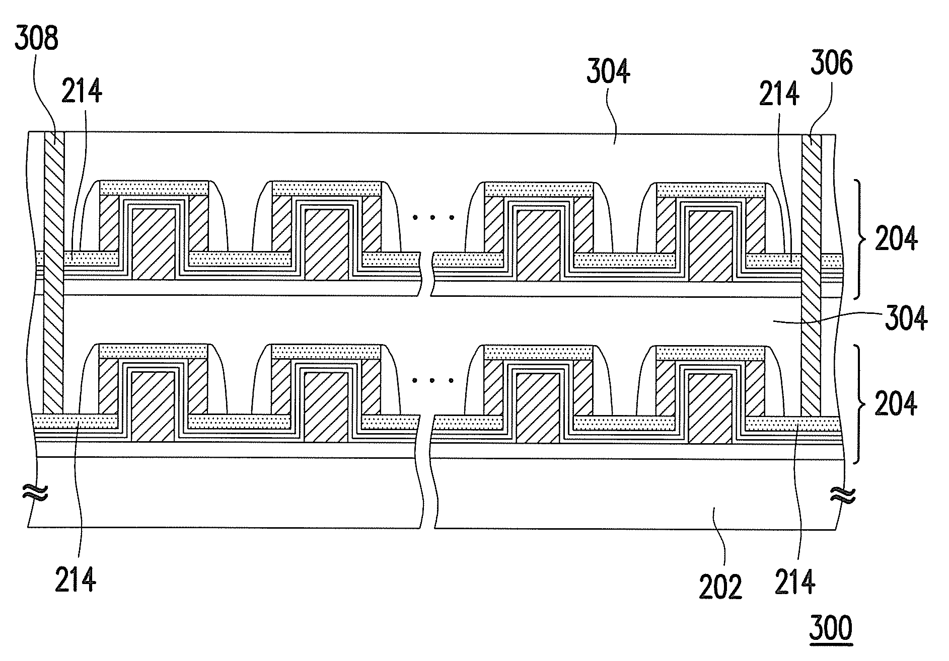
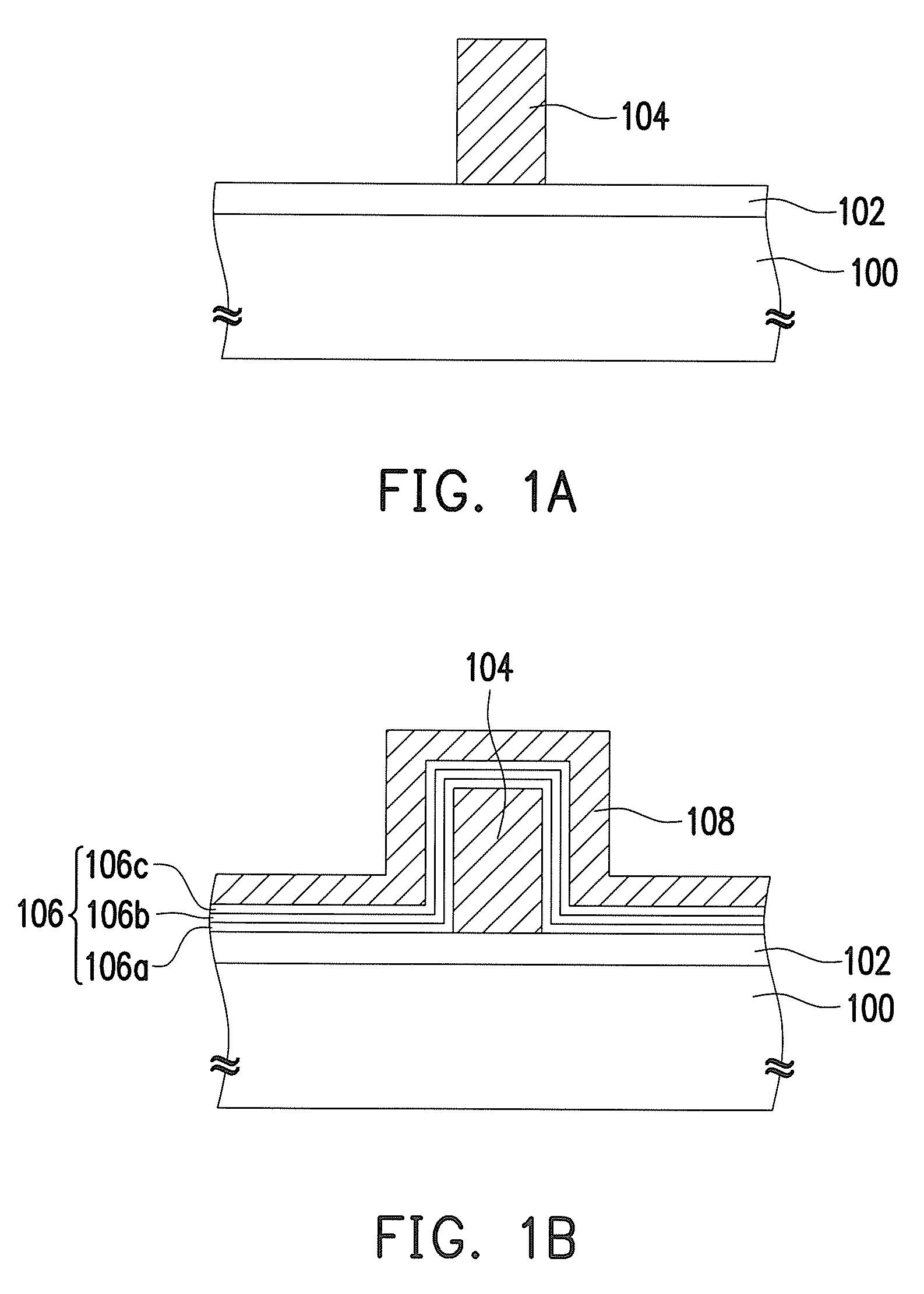
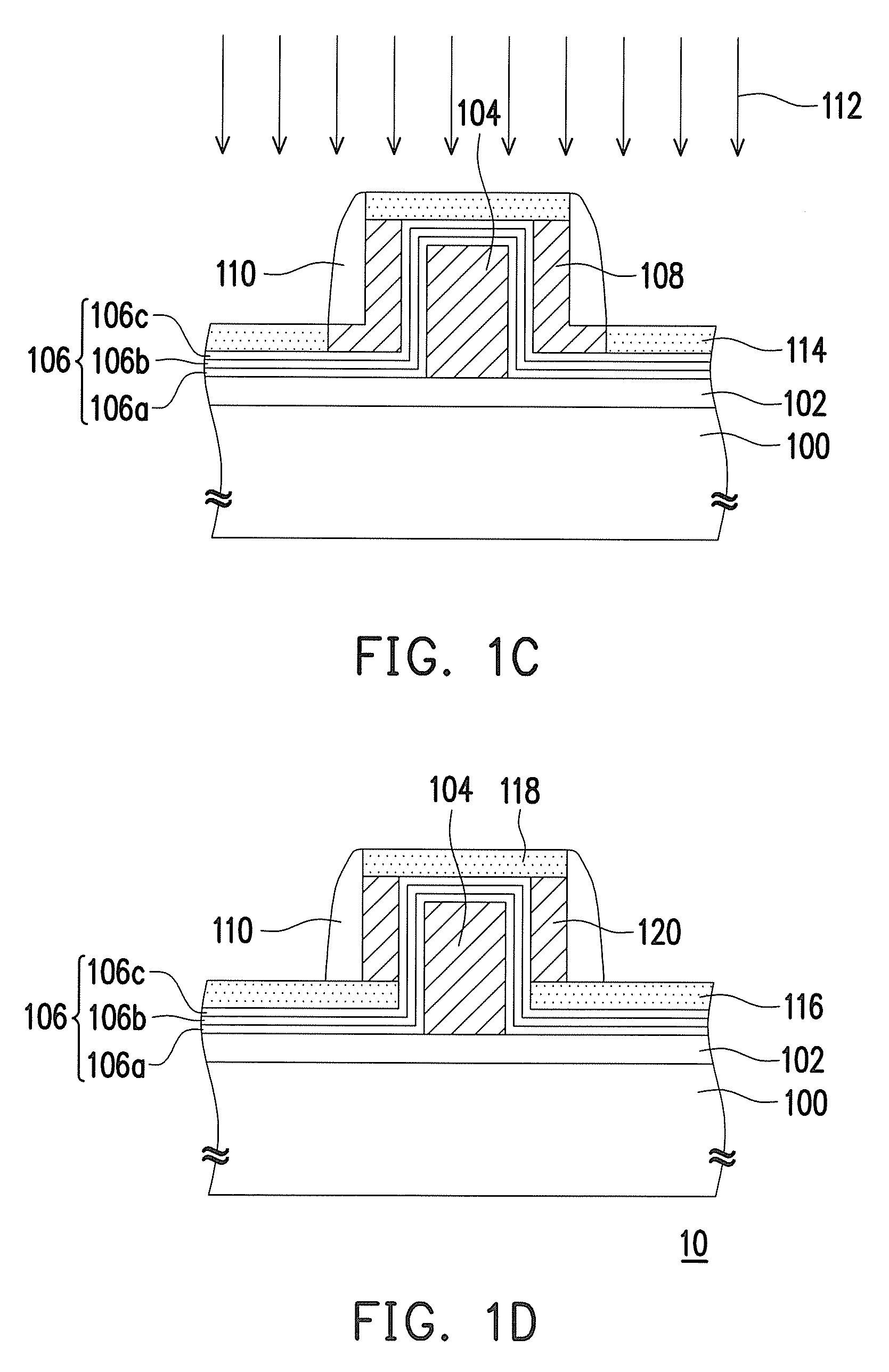
[0036]FIGS. 1A-1D are cross sectional views illustrating a flow diagram of manufacturing a memory cell according to an embodiment of the invention. Referring to FIG. 1A, a substrate 100 is provided. The substrate 100 is, for example, a silicon substrate. Then, an isolation layer 102 is formed over the substrate 100. A method of forming the isolation layer 102 is, for example, a chemical vapor deposition (CVD). A material of the isolation layer 102 is oxide or nitride, for instance. A gate 104 is formed over the isolation layer 102. In a method of forming the gate 104, an undoped polysilicon layer is deposited over the isolation layer 102, and a patterning process is performed, for instance. In addition, after the undoped polysilicon layer is deposited and before the patterning process is performed, an ion implantation process is further performed to implant a P-type dopant into the polysilicon layer.

[0037]Thereafter, referring to FIG. 1B, a charge storage structure 106 is formed ove...


PUM


Abstract

A memory cell is provided. The memory cell includes a substrate, an isolation layer, a gate, a charge storage structure, a first source/drain region, a second source/drain region and a channel layer. The isolation layer is disposed over the substrate. The gate is disposed over the isolation layer. The charge storage structure is disposed over the isolation layer and the gate. The first source/drain region is disposed over the charge storage structure at two sides of the gate. The second source/drain region is disposed over the charge storage structure at top of the gate. The channel layer is disposed over the charge storage structure at sidewall of the gate and is electrically connected with the first source/drain region and the second source/drain region.

Description

BACKGROUND OF THE INVENTION[0001]1. Field of the Invention[0002]The invention relates to a memory cell, a manufacturing method thereof and a memory structure, and more particularly to a memory cell, a manufacturing method thereof and a memory structure capable of reducing an occurrence of punch-through phenomenon and having superior channel boosting capability.[0003]2. Description of Related Art[0004]A memory is a semiconductor device designed for storing information or data. As the functions of computer microprocessors become more and more powerful, programs and operations executed by software are increased correspondingly. As a consequence, the demand for high storage capacity memories is getting higher. The challenge of fabricating memories with large storage capacity and low manufacturing cost to satisfy such a demand is now a driving force for developing the techniques and processes of manufacturing highly integrated semiconductor devices.[0005]Among various types of memory pro...

Claims


Application Information

Patent Timeline
Patent Type & Authority Applications(United States)
IPC IPC(8): H01L29/792H01L21/336
CPCH01L21/28273H01L21/28282H01L27/11551H01L27/11556H01L29/7923H01L29/4983H01L29/66825H01L29/66833H01L29/7887H01L27/11578H01L29/40114H01L29/40117H10B41/20H10B41/27H10B43/20
Inventor HUANG, JYUN-SIANGTSAI, WEN-JEROU, TIEN-FANCHENG, CHENG-HSIEN
Owner MACRONIX INT CO LTD
Why Eureka
Try Eureka