
Led comprising a conductive transparent polymer layer with low sulfate and high metal ion content

a polymer layer and transparent polymer technology, applied in the direction of non-metal conductors, conductors, thermoelectric devices, etc., can solve the problems complex and expensive methods of making layers with conductive and non-conductive areas, and pixels, which are electrically connected via ctp layers, suffer from shrinkage under multipled driving, etc., to achieve the effect of reducing the performance of leds, preventing substantial absorption of visible light, and essentially

Inactive Publication Date: 2003-07-01
KONINKLIJKE PHILIPS ELECTRONICS NV
View PDF6 Cites 41 Cited by
  • Summary
  • Abstract
  • Description
  • Claims
  • Application Information

AI Technical Summary

Benefits of technology

LEDs comprising a conductive transparent polymer are known in the art to increase the lifetime of polymer LEDs essentially. LEDs with CTP layers have been described, for instance, in patent application WO 96 / 08047. Various polymeric materials have been described as suitable for use in LEDs as materials that on the one hand provide areas of electric insulation, and at the other hand provide electroconductive areas that serve as real hole-injection anodes. Such polymers that, depending on the location, can be in the conductive and non-conductive state, have been found in the classes of polythiophenes, polyamines, polypyrroles, polyanilines, and polyacetylenes, which polymers may be substituted with alkyl and alkoxy groups, halogens, and the like. The thickness of these CTP layers is reported to be between 50 and 500 nm. Thin layers are preferred to prevent substantial absorption of the visible light, which decreases the performance of the LED. However, in practice these layers must be relatively thick to prevent leakage currents, short-circuit, and pinholes, and to improve the device lifetime.
Dependent upon the preparation of the conjugated polymer, said polymer may comprise 5 to 10% non-conjugated units. It has been found that such non-conjugated units increase the electroluminescence efficiency, which is defined by the number of photons per injected electron in the active layer.

Problems solved by technology

Thin layers are preferred to prevent substantial absorption of the visible light, which decreases the performance of the LED.
The major disadvantage of these CTP layers is the complicated and expensive method of making layers with conductive and non-conductive areas, e.g. for use in a matrix or segmented organic LED displays.
Such pixels, which are electrically connected via the CTP layer suffer from shrinkage under multipled driving.

Method used


Image

  • Led comprising a conductive transparent polymer layer with low sulfate and high metal ion content
  • Led comprising a conductive transparent polymer layer with low sulfate and high metal ion content
  • Led comprising a conductive transparent polymer layer with low sulfate and high metal ion content

Examples


example 2

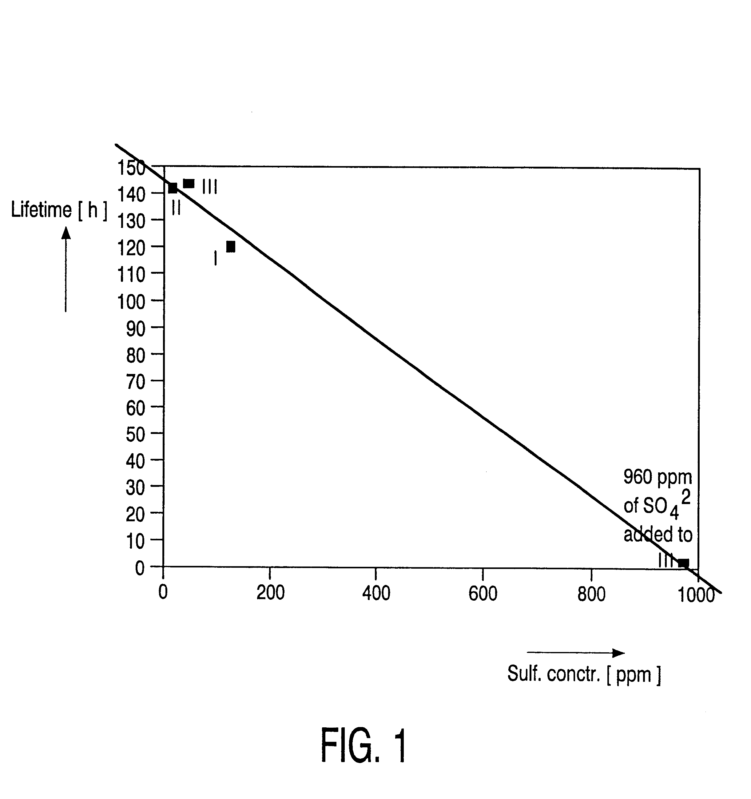
Example 1 was repeated, except that different concentrations of sulfate ions were added to the PEDOT dispersion. To demonstrate that SO.sub.4.sup.2- ions are detrimental to lifetime and efficiency of a polyLED, sulfuric acid (H.sub.2 SO.sub.4) was added to PEDOT:

A 100 ml of the PEDOT dispersion of Example 1 has a 4 wt. % solid content, of which about 95 wt. % is PSS. This corresponds to 0.021 mole monomer of PSS in 100 ml of PEDOT.

Respectively, 0.001 mole (=0.096 g=960 ppm SO.sub.4.sup.2- per 100 ml) and 0.005 moles (=0.48 g=4800 ppm SO.sub.4.sup.2- per 100 ml) of H.sub.2 SO.sub.4 were added to the PEDOT dispersion. The efficiency and lifetime of the devices decreased dramatically as shown in Table 2.

Metal ion sulfates, such as K.sub.2 SO.sub.4, added to the PEDOT dispersion had the same detrimental effect as H.sub.2 SO.sub.4.

Table 2. Efficiency at room temperature and lifetime under DC driving of the light emitting polymer at 80.degree. C., 200 cd / m.sup.2 with standard and modified...

example 3

Example 1 was repeated, except that NaCl was added to the PEDOT dispersion to prevent anode shrinkage as presented in FIG. 4, to give 0.022 mmoles / g of sodium in the dispersion. The material as used in Example 1 showed an inhomogeneous electroluminescence in four rows of pixels already after 24 h at 80.degree. C. under multiplexed driving, whereas the matrix display in addition containing 0.022 mmoles / g of sodium did not give anode shrinkage after 24 h.

example 4

Example 1 was repeated, except that NaCl was added to the PEDOT dispersion to give 0.088 mmoles / g of sodium in the dispersion. After 96 h service lifetime test under a multiplexed driving scheme, the matrix display showed no anode shrinkage.

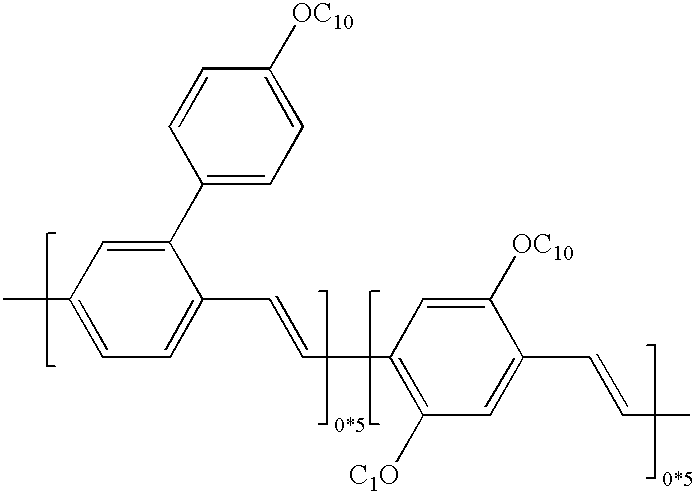
The examples hereinabove illustrate that the amount of sodium in a charge transport polymer (CTP) layer for use in an organic LED may have a significant effect on the extent of anode shrinkage observed in accelerated service life tests in which the LED is driven in a multiplexed driving scheme. The light emitting polymer used is these examples is a PPV.

Similar results are obtained for polyfluorenes as light emitting polymer. In a specific example of a LED comprising a red emitting polyfluorene and a CTP layer comprising about 0.25 mmol / g Na, no anode shrinkage is observed in a lifetime test performed at 80.degree. C. for 600 h. By comparison, if the same CTP layer is used but without sodium severe anode shrinkage is observed. Identical results ar...


PUM

PropertyMeasurementUnit
thicknessaaaaaaaaaa
thicknessaaaaaaaaaa
thicknessaaaaaaaaaa

Abstract

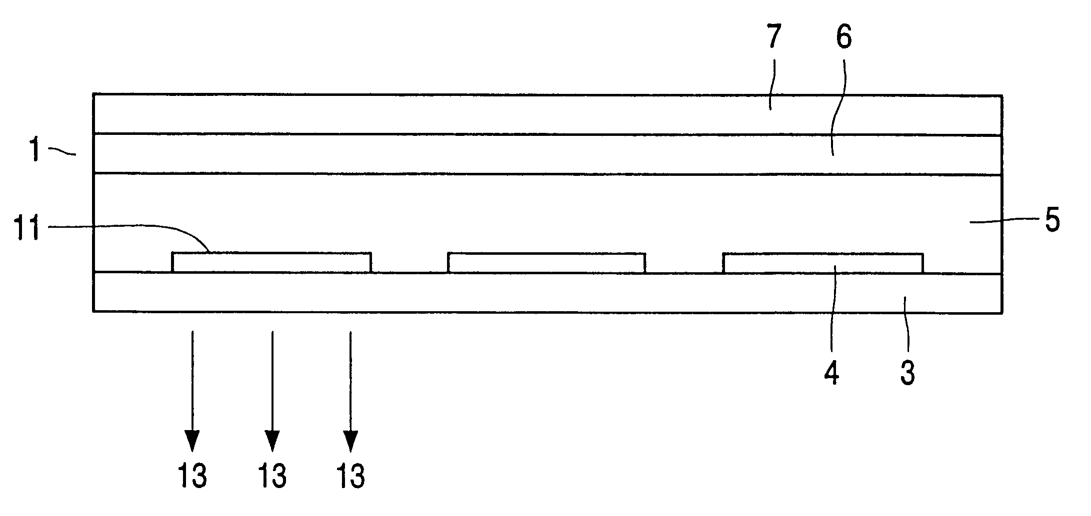
The invention pertains to an organic light emitting diode (LED) comprising a transparent electrode, superposed by a layer of a conductive transparent polymer (CTP), superposed by a layer of a light emitting polymer, oligomer, or low molecular weight compound superposed by a metal cathode, characterized in that the CTP layer has a sulfate ion content of less than 7,500 ppm, and a metal ion content of more than 0.04 mmoles / g.

Description

FIELD TECHNOLOGYThe invention pertains to an organic light emitting diode (LED) comprising a transparent electrode, superposed by a layer of a conductive transparent polymer (CTP), superposed by a layer of a light emitting polymer, oligomer, or low molecular weight compound, superposed by a metal cathode, wherein the CTP layer has a low sulfate and high metal ion content.BACKGROUND AND SUMMARYLEDs comprising a conductive transparent polymer are known in the art to increase the lifetime of polymer LEDs essentially. LEDs with CTP layers have been described, for instance, in patent application WO 96 / 08047. Various polymeric materials have been described as suitable for use in LEDs as materials that on the one hand provide areas of electric insulation, and at the other hand provide electroconductive areas that serve as real hole-injection anodes. Such polymers that, depending on the location, can be in the conductive and non-conductive state, have been found in the classes of polythioph...

Claims


Application Information

Patent Timeline
Patent Type & Authority Patents(United States)
IPC IPC(8): C09K11/06H01B1/12H01L51/52H01L51/05H01L51/30H01L51/50H05B33/28H10K99/00
CPCC09K11/06H01B1/128H01L51/0037H01L51/5088C09K2211/1408C09K2211/1425H01L51/0038H10K85/114H10K85/1135H10K50/17H05B33/26H05B33/28
Inventor BUECHEL, MICHAELJACOBS, BOUDEWIJN JOHANNES CATHARINUSGREUEL, GEORGDE KOK VAN BREEMEN, MARGARETHA MARIAVAN DE WEIJER, PETER
Owner KONINKLIJKE PHILIPS ELECTRONICS NV
Learn More