Manufacture method of array substrate, array substrate and display device

A technology of array substrates and substrates, which is applied in the manufacture of array substrates, array substrates and display devices, can solve the problems of increased manufacturing costs during manufacturing time, achieve the effects of reducing signal delay, reducing process time, and improving display quality

Inactive Publication Date: 2012-08-22
BOE TECH GRP CO LTD +1
View PDF5 Cites 38 Cited by
  • Summary
  • Abstract
  • Description
  • Claims
  • Application Information

AI Technical Summary

Problems solved by technology

In the existing method for improving signal delay, the parasitic capacitance is mainly reduced by increasing the thickness of the protective f

Method used


Image

  • Manufacture method of array substrate, array substrate and display device
  • Manufacture method of array substrate, array substrate and display device
  • Manufacture method of array substrate, array substrate and display device

Examples


Example Embodiment

[0091] Method Example 1

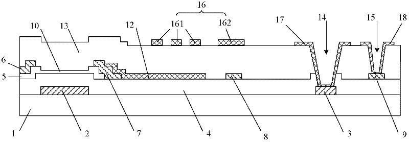
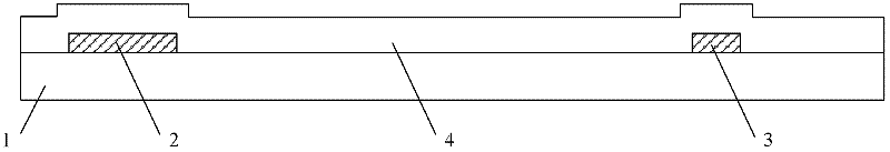
[0092] Step S11, providing a substrate, and forming gate lines, gate electrodes and gate pads on the substrate;

[0093] First, sputtering, thermal evaporation or other film forming methods can be used to form a gate metal layer on a glass substrate or other type of transparent substrate. The gate metal layer can be made of chromium (Cr), molybdenum (Mo), aluminum (Al), Copper (Cu), tungsten (W), neodymium (Nd) and their alloys, and the gate metal layer can be one or more layers; then, a photoresist is formed on the gate metal layer; secondly, a patterned The mask plate exposes and develops the photoresist to form a photoresist mask; again, the photoresist mask is used to etch the gate metal layer to form patterns of gate lines, gate electrodes and gate pads; finally, Strip the remaining photoresist. It should be noted that, in this step, when the patterns of the gate line, the gate electrode and the gate pad are formed, a common electrode line may also ...

Example Embodiment

[0120] Method Example 2

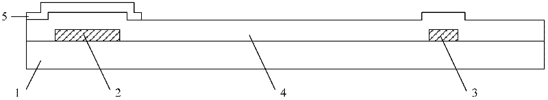
[0121] Step S21, providing a substrate, and forming gate lines, gate electrodes and gate pads on the substrate;

[0122] First, sputtering, thermal evaporation or other film forming methods can be used to form a gate metal layer on a glass substrate or other type of transparent substrate. The gate metal layer can be made of chromium (Cr), molybdenum (Mo), aluminum (Al), Copper (Cu), tungsten (W), neodymium (Nd) and their alloys, and the gate metal layer can be one or more layers; then, a photoresist is formed on the gate metal layer; secondly, a patterned The mask plate exposes and develops the photoresist to form a photoresist mask; again, the photoresist mask is used to etch the gate metal layer to form patterns of gate lines, gate electrodes and gate pads; finally, Strip the remaining photoresist. It should be noted that, in this step, when the patterns of the gate line, the gate electrode and the gate pad are formed, a common electrode line may also ...


PUM


Abstract

The invention provides a manufacture method of an array substrate, the array substrate and a display device. A display region of the array substrate comprises a gate line, a data line and a plurality of pixel units. A non-display region comprises a gate bonding pad and a data bonding pad. Each of the pixel units comprises a thin film transistor, a pixel electrode and a common electrode. The pixel electrode is connected to a drain electrode of the thin film transistor. The common electrode comprises a first common electrode arranged above the pixel electrode and a second common electrode arranged above the data line. A protective film is arranged between a common electrode layer and a pixel electrode layer. An inorganic insulating film and an organic insulating film are arranged between the pixel electrode and the data line and between the thin film transistor and the protective film, respectively. The inorganic insulating film is formed above the data line, a source and the drain of the thin film transistor, and a semiconductor layer of a channel region, and the organic insulating film is arranged above the inorganic insulating film. The invention can reduce signal delay on the data line, and prevent generation of leakage current in the thin film transistor at a high temperature.

Description

technical field [0001] The invention relates to the field of liquid crystal display, in particular to a method for manufacturing an array substrate, the array substrate and a display device. Background technique [0002] Thin film transistor liquid crystal display (TFT-LCD) has the characteristics of small size, low power consumption, and no radiation, and occupies a dominant position in the current flat panel display market. Among them, ADvanced Super Dimension Switch (ADS for short), through the electric field generated by the edge of the slit electrode in the same plane and the electric field generated between the slit electrode layer and the plate electrode layer, forms a multi-dimensional electric field, making the liquid crystal All oriented liquid crystal molecules between the slit electrodes in the cell and directly above the electrodes can be rotated, thereby improving the working efficiency of the liquid crystal and increasing the light transmission efficiency. Ad...

Claims


Application Information

Patent Timeline
IPC IPC(8): G02F1/1362G02F1/1368G02F1/1343H01L21/77
CPCG02F1/134363G02F1/1362
Inventor 金玟秀邓立赟周纪登
Owner BOE TECH GRP CO LTD
Why Eureka
Try Eureka