OLED display panel and manufacturing method thereof

A technology for display panels and manufacturing methods, applied in semiconductor/solid-state device manufacturing, organic semiconductor devices, electrical components, etc., can solve problems such as threshold voltage offset, offset, and influence on TFT characteristics, so as to prevent light leakage current and ensure characteristics, the effect of maintaining normal operation

Active Publication Date: 2017-09-15
WUHAN CHINA STAR OPTOELECTRONICS SEMICON DISPLAY TECH CO LTD
View PDF4 Cites 42 Cited by
  • Summary
  • Abstract
  • Description
  • Claims
  • Application Information

AI Technical Summary

Problems solved by technology

However, the IGZO active layer in the IGZO-TFT is very sensitive to the process and environment. Since the band gap of IGZO (about 3.4eV) is similar to that of ultraviolet (UV) light (higher than 3.1eV), IGZO is sensitive to UV light. It has a good absorption effect. Under the irradiation of UV light, the IGZO active layer easily absorbs energy such as electrons in the valence band and jumps to the conduction band, which shifts the threshold voltage of TFT and causes the display effect to be unstable.
Therefore, in the traditional top gate (top gate) IGZO-TFT manufacturing process, in order to prevent the IGZO active layer of the driver TFT from being affected by the light from the bottom of the TFT to generate light leakage current, a blocking layer is usually made at the bottom of the TFT. The light-shielding (shielding) metal layer, but for the bottom emission OLED (bottom emission-OLED) display panel, the IGZO active layer will be affected by the light incident from the top of the TFT, thereby inducing the active layer to generate light leakage current, affecting the TFT The characteristics of the TFT may even cause a shift in the threshold voltage Vth of the TFT, affecting the normal operation of the TFT

Method used


Image

  • OLED display panel and manufacturing method thereof
  • OLED display panel and manufacturing method thereof
  • OLED display panel and manufacturing method thereof

Examples


Embodiment Construction

[0040] In order to further illustrate the technical means adopted by the present invention and its effects, the following describes in detail in conjunction with preferred embodiments of the present invention and accompanying drawings.

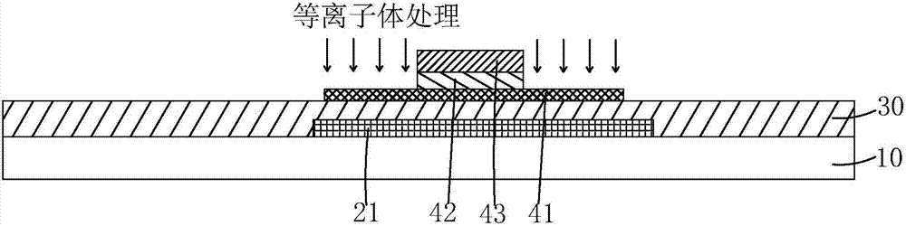
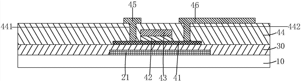
[0041] see Figure 5 The present invention firstly provides an OLED display panel, comprising a base substrate 10, a light-shielding metal block 21 disposed on the base substrate 10, a buffer layer 30 disposed on the light-shielding metal block 21 and the base substrate 10, and On the buffer layer 30 and corresponding to the active layer 41 above the light-shielding metal block 21 , the gate insulating layer 42 disposed on the active layer 41 , the gate disposed on the gate insulating layer 42 43. The interlayer insulating layer 44 disposed on the gate 43, the active layer 41 and the buffer layer 30, disposed on the interlayer insulating layer 44 and corresponding to the first pass on both sides of the active layer 41 The hole 441 and the sec...


PUM


Abstract

The invention provides an OLED display panel and a manufacturing method thereof. Through arranging a red light-shielding color block which totally covers an active layer above an IGZO TFT, influence of high-energy blue light which is incident from top of the IGZO TFT to the active layer of IGZO can be reduced, thereby preventing generation of photogenerated leakage current, ensuring characteristics of the IGZO TFT, and sustaining normal operation of the IGZO TFT. Furthermore because the red light-shielding color block which covers the active layer only blocks the high-energy shortwave blue light which affects the active layer of the IGZO TFT, the light in other wave bands can penetrate through normally, aperture rate of the light emitting area of the OLED display panel is not affected.

Description

technical field [0001] The invention relates to the field of display technology, in particular to an OLED display panel and a manufacturing method thereof. Background technique [0002] With the development of display technology, flat display devices such as Liquid Crystal Display (LCD) and Organic Light-Emitting Diode (OLED) display have become the mainstream of display devices. Among them, organic light-emitting diode display, also known as organic electroluminescence display, is an emerging flat panel display device, due to its simple preparation process, low cost, low power consumption, high luminous brightness, wide range of operating Thin and light, fast response, easy to realize color display and large-screen display, easy to realize matching with integrated circuit driver, easy to realize flexible display, etc., so it has broad application prospects. [0003] According to the driving method, OLED displays can be divided into two categories: passive matrix OLED (Pass...

Claims


Application Information

Patent Timeline
Patent Type & Authority Applications(China)
IPC IPC(8): H01L27/12H01L27/32H01L21/77
CPCH01L27/1225H01L27/1259H10K59/12H10K59/126H01L29/78633H01L29/7869H01L29/66969H10K59/38H10K59/1201H10K71/00H01L27/1248H10K59/122H10K59/1213H10K50/81H10K50/82H10K50/84H10K2102/103
Inventor 李松杉
Owner WUHAN CHINA STAR OPTOELECTRONICS SEMICON DISPLAY TECH CO LTD
Why Eureka
Try Eureka