Semiconductor device and preparation method thereof

A semiconductor and device technology, applied in the field of semiconductor devices and their preparation, can solve the problems of reduced threshold voltage stability of memory arrays, lengthy process steps and process steps, affecting component performance and reliability, etc., so as to reduce device area and increase Effective channel length, effect of overcoming short channel effect

Pending Publication Date: 2020-03-27
CHANGXIN MEMORY TECH INC
View PDF0 Cites 1 Cited by
  • Summary
  • Abstract
  • Description
  • Claims
  • Application Information

AI Technical Summary

Problems solved by technology

[0002] A vertical surrounding gate transistor (SGT) with a buried bit line, which uses increased isolation rules to greatly reduce the difficulty of shallow trench isolation manufacturing, and its process includes lengthy buried bit lines The process steps, the process steps of the spin-on dielectric layer (SOD), the process steps of metal and N-type doped polysilicon to define the gate length of the transistor, the process is complicated, and the stability of the threshold voltage of the memory array is also significantly reduced. , and under the limitation of the vertical size, it is impossible to reduce the change of the threshold voltage (Vth) with a longer channel length
[0003] In addition, due to the continuous miniaturization of the size of semiconductor devices, the distance between the memory cells of the dynamic random access memory (DRAM) is also closer, which often leads to a very strong word line-word line coupling effect (word line-word line-coupling effect). word line coupling), which will affect device performance and reliability, and even cause DRAM data access errors

Method used


Image

  • Semiconductor device and preparation method thereof
  • Semiconductor device and preparation method thereof
  • Semiconductor device and preparation method thereof

Examples


Embodiment Construction

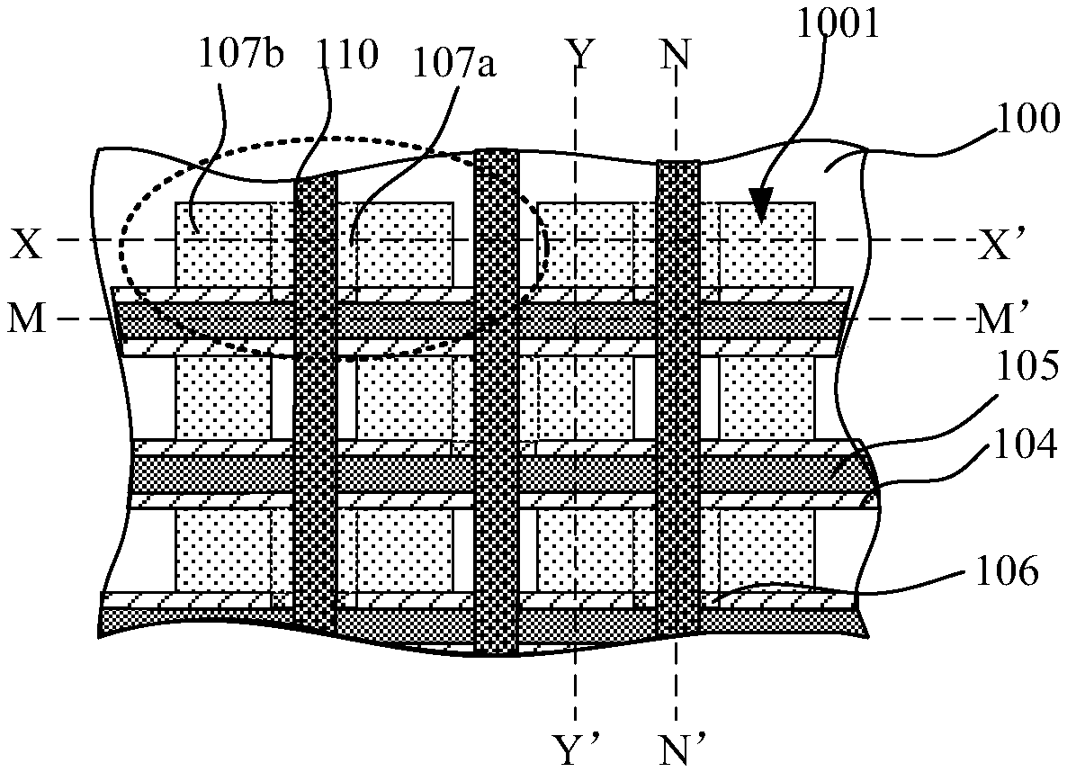
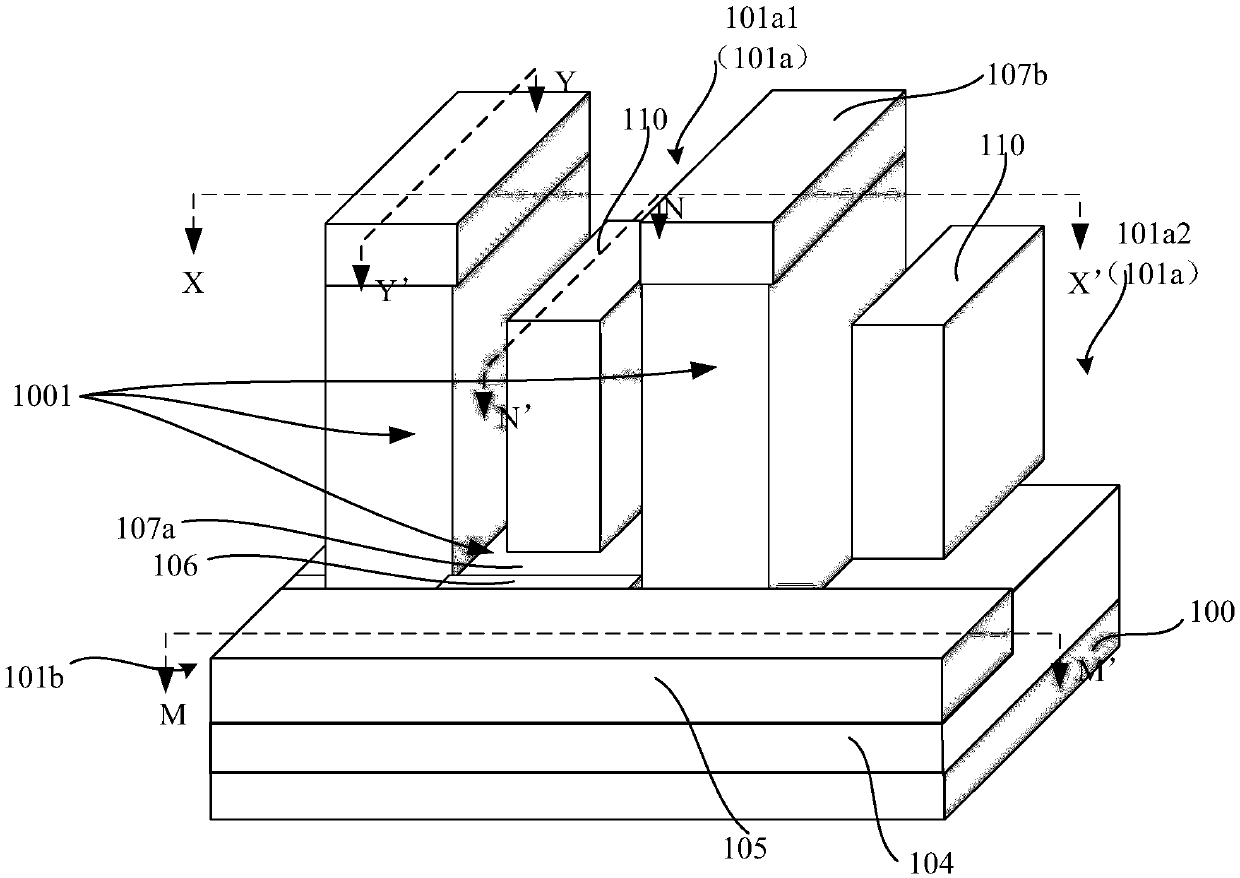
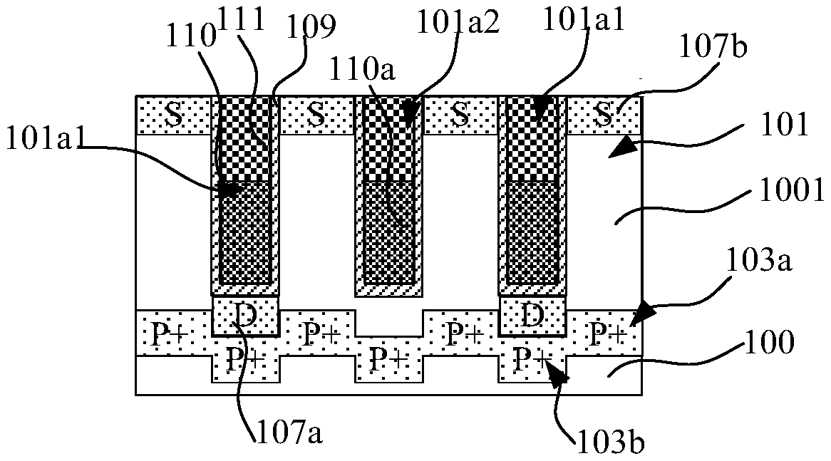
[0080] In order to make the purpose and features of the present invention more obvious and understandable, the technical solutions of the present invention will be described in detail below in conjunction with the accompanying drawings. However, the present invention can be implemented in different forms and should not be limited to the described embodiments. It should be noted that the "semiconductor substrate on both sides of the first trench" herein refers to the region where the first trench does not intersect with the second trench (that is, the area where the first trench does not intersect with the second trench). The semiconductor substrate on both sides of the area other than the intersection with the second trench); the "semiconductor substrate at the bottom of the first trench" herein means that the first trench is not connected to the first trench. The region where the two trenches intersect the bottom of the semiconductor substrate. Furthermore, it should be readi...


PUM


Abstract

The invention provides a semiconductor device and a preparation method thereof. A second trench extending along a second direction is formed in a semiconductor substrate. U-shaped fins are arranged onthe two sides of the second trench in a staggered mode. The U-shaped fin is provided with a first trench extending along a first direction. The first source / drain regions are formed in the fins at the tops of the two sides of the first trench; a second source / drain region is formed in the fin at the bottom of the first trench; a gate line is filled in the first trench and extends along the firstdirection; the embedded wire is filled in the second trench extending along the second direction, so that the two first source / drain regions in the U-shaped fin respectively form double vertical L-shaped channels with the second source / drain region, the effective channel length is favorably increased, the short channel effect is overcome, and the smaller feature size and the higher integration degree are further favorably realized; and the U-shaped fins on the two sides of the second trench are arranged in a staggered manner, so that the coupling effect between adjacent active regions can be improved, and the device performance can be improved.

Description

technical field [0001] The invention relates to the technical field of integrated circuit manufacturing, in particular to a semiconductor device and a preparation method thereof. Background technique [0002] A vertical surrounding gate transistor (SGT) with a buried bit line, which uses increased isolation rules to greatly reduce the difficulty of shallow trench isolation manufacturing, and its process includes lengthy buried bit lines The process steps, the process steps of the spin-on dielectric layer (SOD), the process steps of metal and N-type doped polysilicon to define the gate length of the transistor, the process is complicated, and the stability of the threshold voltage of the memory array is also significantly reduced. , and under the limitation of the vertical size, it is impossible to reduce the change of the threshold voltage (Vth) with a longer channel length. [0003] In addition, due to the continuous miniaturization of the size of semiconductor devices, th...

Claims


Application Information

Patent Timeline
Patent Type & Authority Applications(China)
IPC IPC(8): H01L29/78H01L21/336H01L29/423H01L29/10
CPCH01L29/1037H01L29/4236H01L29/66477H01L29/785
Inventor 不公告发明人
Owner CHANGXIN MEMORY TECH INC
Why Eureka
Try Eureka