MOSFET structure

A channel region and substrate technology, applied in the direction of electrical components, circuits, semiconductor devices, etc., can solve the problems that the peak value of the electric field on the channel surface cannot be effectively reduced, and the short channel effect of semiconductor devices cannot be overcome, so as to increase the effective channel of the device. channel length, suppression of short channel effects, and enhanced controllability

Inactive Publication Date: 2017-09-22
NANJING UNIV OF POSTS & TELECOMM
View PDF9 Cites 1 Cited by
  • Summary
  • Abstract
  • Description
  • Claims
  • Application Information

AI Technical Summary

Problems solved by technology

[0008] The technical problem to be solved by the present invention is to overcome the deficiencies of the prior art, provide a MOSFET structure, and solve the problem that the existing MOS transistor cannot overcome the short channel effect in the semiconductor device structurally, and cannot effectively reduce the peak value of the electric field on the surface of the channel. The problem

Method used


Image

  • MOSFET structure
  • MOSFET structure
  • MOSFET structure

Examples


Embodiment Construction

[0029] Embodiments of the present invention will be described below in conjunction with the accompanying drawings.

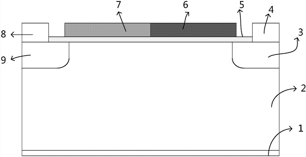
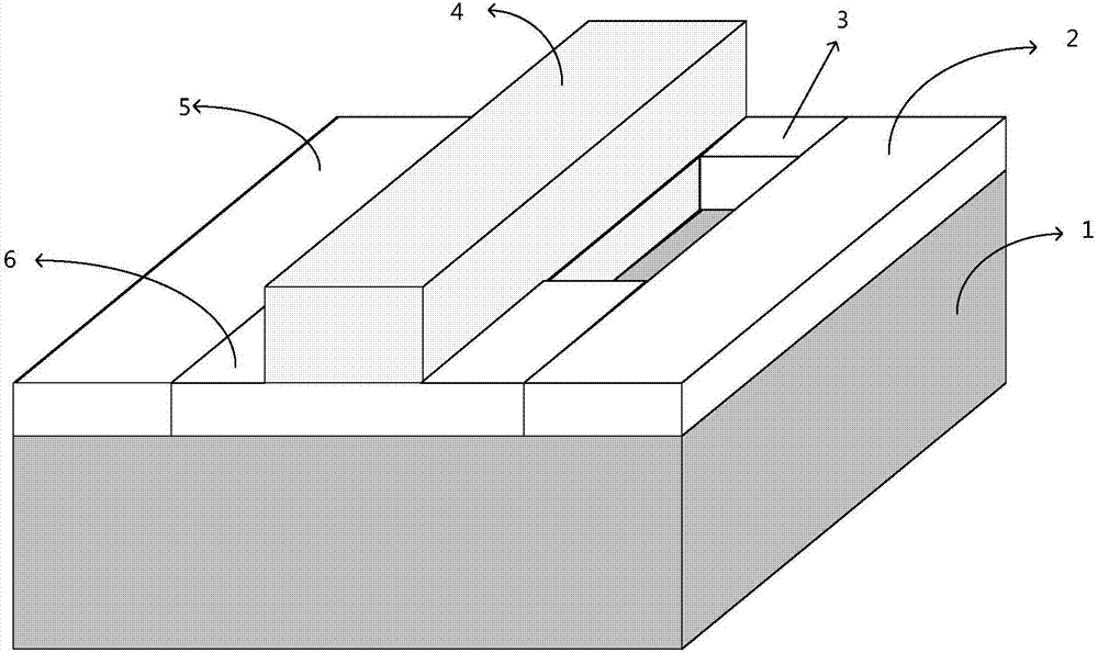
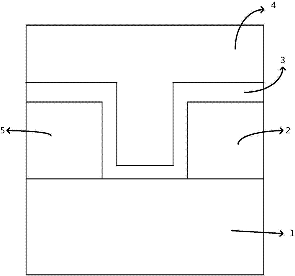
[0030] The invention designs a MOSFET structure, which comprises a substrate electrode, a substrate, a channel region, a source region, a drain region, a source electrode, a drain electrode, a gate oxide layer and a gate. On this basis, the present invention forms the substrate region built into the substrate into a channel region with a non-planar surface, and the two sides of the channel region are respectively provided with a source region and a drain region composed of semiconductor regions; the source The electrode and the drain are arranged on the source region and the drain region respectively; the gate oxide layer covers the surface of the non-planar channel region; the gate is arranged on the surface of the gate oxide layer, and the two ends of the gate are connected to the source There are gaps between the gate and the drain, and the two ends of the ga...


PUM


Abstract

The invention discloses a MOSFET structure which belongs to the technical field of semiconductor devices and comprises a substrate electrode, a substrate, a channel region, a source region, a drain region, a source electrode, a drain electrode, a gate oxide layer and a gate electrode. The channel region with a non-planar surface is formed in a substrate region built in the substrate, and the source region and the drain region are arranged on both sides of the channel region respectively. The source electrode and the drain electrode are correspondingly arranged in the source region and the drain region respectively. The gate oxide layer covers the surface of the non-planar channel region. The gate electrode is arranged on the surface of the gate oxide layer, and both ends of the gate electrode are spaced from the source electrode and the drain electrode. Both ends of the gate electrode respectively extend to the source region and the drain region to form overlap. According to the invention, the non-planar channel MOSFET structure is used to reduce the electric field peak of the drain region and increase the effective channel length of a device; a leakage-induced barrier reducing effect is improve and suppressed; a short channel effect is suppressed; the high electric field of the drain region is reduced; the generation of hot carriers is suppressed; and the stability of the device is improved.

Description

technical field [0001] The invention relates to a MOSFET structure and belongs to the technical field of semiconductor devices. Background technique [0002] With the rapid development of the semiconductor industry, the scale of integrated circuits continues to increase, which requires the continuous reduction of device size, and the reduction of device size will inevitably bring about the short channel effect, that is, a series of performance shifts caused by the shortening of the device channel length . The short channel effect mainly brings the following effects: [0003] The threshold voltage is no longer a constant, it will change with the change of the channel length; the strong electric field in the drain region will lead to the reduction of the barrier of the source region, resulting in the deterioration of the subthreshold characteristics of the device, and the device cannot be completely turned off; The shortening of the channel will lead to the formation of a hi...

Claims


Application Information

Patent Timeline
Patent Type & Authority Applications(China)
IPC IPC(8): H01L29/78H01L29/08H01L29/10H01L29/423
CPCH01L29/0847H01L29/1037H01L29/42364H01L29/78
Inventor 郭宇锋张茂林姚佳飞李曼王子轩潘志刚
Owner NANJING UNIV OF POSTS & TELECOMM
Why Eureka
Try Eureka