HEMT device with multi-metal gate structure and preparation method thereof

A metal structure and gate structure technology, applied in the fields of semiconductor/solid-state device manufacturing, semiconductor devices, electrical components, etc., can solve the problems of poor repeatability, difficult and precise control of electron beam deposition, etc., to improve the breakdown voltage and improve the dynamic performance. Effect

Pending Publication Date: 2020-07-10
ZHONGSHAN INST OF MODERN IND TECH SOUTH CHINA UNIV OF TECH +1
View PDF0 Cites 3 Cited by
  • Summary
  • Abstract
  • Description
  • Claims
  • Application Information

AI Technical Summary

Problems solved by technology

However, the above-mentioned method of changing the angle of electron beam deposition is difficult to control accurately and has poor repeatability

Method used


Image

  • HEMT device with multi-metal gate structure and preparation method thereof
  • HEMT device with multi-metal gate structure and preparation method thereof
  • HEMT device with multi-metal gate structure and preparation method thereof

Examples


Embodiment 1

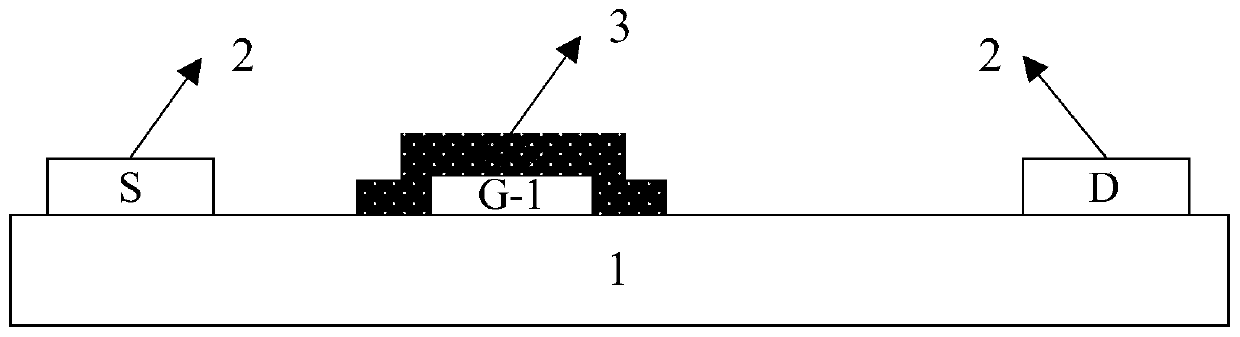
[0029] This embodiment provides a HEMT device with a multi-metal gate structure, such as image 3 As shown, the device includes an AlGaN / GaN epitaxy 1, the two ends of the upper surface of the AlGaN / GaN epitaxy are respectively connected to the source and drain electrodes 2, and the source and drain electrodes 2 are provided with a gate electrode 3 near the source side, and the gate electrode 3 is the first A layer of metal Ti is deposited by electron beam evaporation, and the second layer of metal Ni of the gate electrode 3 is deposited by magnetron sputtering without additional photolithography steps. The contact metal structure is Ni / Ti / Ni. image 3 G-1 in represents the first layer of metal, and G-2 represents the second layer of metal.

[0030] This embodiment also provides a method for preparing a HEMT device with a multi-metal gate structure, comprising the following steps:

[0031] (1) In AlGaN / GaN epitaxy (the epitaxial layer before the source-drain contact electrod...

Embodiment 2

[0035] This embodiment provides a HEMT device with a multi-metal gate structure, such as image 3 As shown, the device includes an AlGaN / GaN epitaxy 1, the two ends of the upper surface of the AlGaN / GaN epitaxy are respectively connected to the source and drain electrodes 2, and the source and drain electrodes 2 are provided with a gate electrode 3 near the source side, and the gate electrode 3 is the first A layer of metal TiN is deposited by electron beam evaporation, and the second layer of metal W of the gate electrode 3 is deposited by magnetron sputtering without additional photolithography steps. The contact metal structure is W / TiN / W.

[0036] This embodiment also provides a method for preparing a HEMT device with a multi-metal gate structure, comprising the following steps:

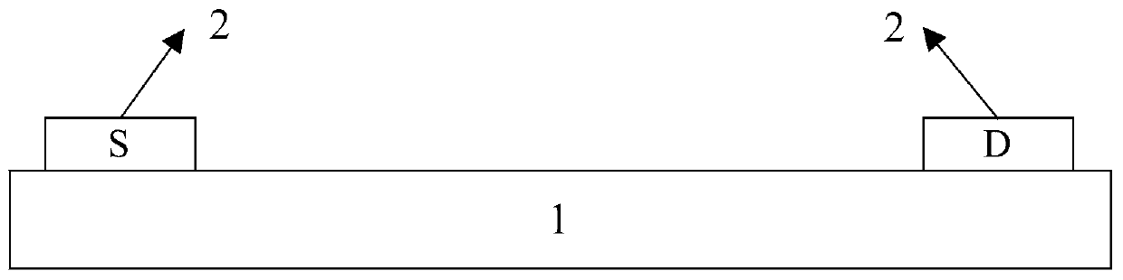
[0037] (1) Define the source-drain electrode window on the AlGaN / GaN epitaxy 1, prepare the source-drain electrode 2 and perform annealing to form an ohmic contact, such as figure 2 shown;

[0...


PUM

PropertyMeasurementUnit
lengthaaaaaaaaaa
lengthaaaaaaaaaa
thicknessaaaaaaaaaa

Abstract

The invention discloses an HEMT device with a multi-metal gate structure and a preparation method thereof. The device comprises an AlGaN/GaN epitaxy layer; the two ends of the upper surface of the AlGaN/GaN epitaxy layer are connected with a source electrode and a drain electrode respectively; a gate electrode is arranged between the source electrode and the drain electrode at the place close to the source electrode side; and a first layer of metal X of the gate electrode is deposited in an electron beam evaporation mode, a second layer of metal Y of the gate electrode is deposited in a magnetron sputtering mode, the work function of the second layer of metal Y of the gate electrode is higher than that of the first layer of metal X, photoetching is not needed, and a metal structure which is formed after the gate electrode is stripped and makes contact with (Al)GaN is Y/X/Y. The multi-metal gate structure is in contact with (Al)GaN, so that the electric field is redistributed, the peakvalue of the electric field at the gate edge near the drain is reduced, and the breakdown voltage of the device is improved; and meanwhile, the lower electric field peak value of the gate edge weakensgate injection electrons to form a virtual gate effect, so that current collapse of the device is reduced, and the dynamic performance of the device is improved.

Description

technical field [0001] The invention relates to the field of semiconductors, in particular to a HEMT device with a multi-metal gate structure and a preparation method thereof. Background technique [0002] GaN materials are widely used in high-frequency power amplifiers and high-voltage power switches due to their high electron mobility, low on-resistance, excellent heat dissipation capability, and high breakdown. At present, the breakdown voltage of GaN-based HEMT devices is far from the theoretical limit of GaN materials (3.4 MV / cm). Devices are often prone to breakdown between the gate and drain. How to reduce the height of the gate edge near the drain? The electric field peak will be beneficial to increase the breakdown voltage of the device. The most common method at present is to use a gate field plate or a source field plate to adjust the electric field distribution, thereby reducing the high electric field peak at the edge of the gate near the drain. On the other h...

Claims


Application Information

Patent Timeline
Patent Type & Authority Applications(China)
IPC IPC(8): H01L29/778H01L29/47H01L29/423H01L21/335
CPCH01L29/42316H01L29/475H01L29/66462H01L29/778
Inventor 王洪高升刘晓艺胡文龙
Owner ZHONGSHAN INST OF MODERN IND TECH SOUTH CHINA UNIV OF TECH
Why Eureka
Try Eureka