Silicon carbide double-groove MOSFET integrated with channel diode

A technology of integrating channels and diodes, applied in electrical components, electro-solid devices, circuits, etc., can solve the problems of bipolar degradation effect, non-deterioration of MOSFET performance, and excessive conduction voltage drop of freewheeling diodes, so as to reduce the electric field. peak value, improved reverse conductivity, and improved reliability

Active Publication Date: 2022-01-28
UNIV OF ELECTRONICS SCI & TECH OF CHINA
View PDF9 Cites 3 Cited by
  • Summary
  • Abstract
  • Description
  • Claims
  • Application Information

AI Technical Summary

Problems solved by technology

[0004] The purpose of the present invention is to address the above problems, and propose a silicon carbide double-slot MOSFET with integrated channel diodes, which can avoid the excessive conduction voltage drop of the freewheeling diode and the bipolar degradation effect while ensuring that the original performance of the MOSFET does not decline. two questions

Method used


Image

  • Silicon carbide double-groove MOSFET integrated with channel diode
  • Silicon carbide double-groove MOSFET integrated with channel diode

Examples


Embodiment 1

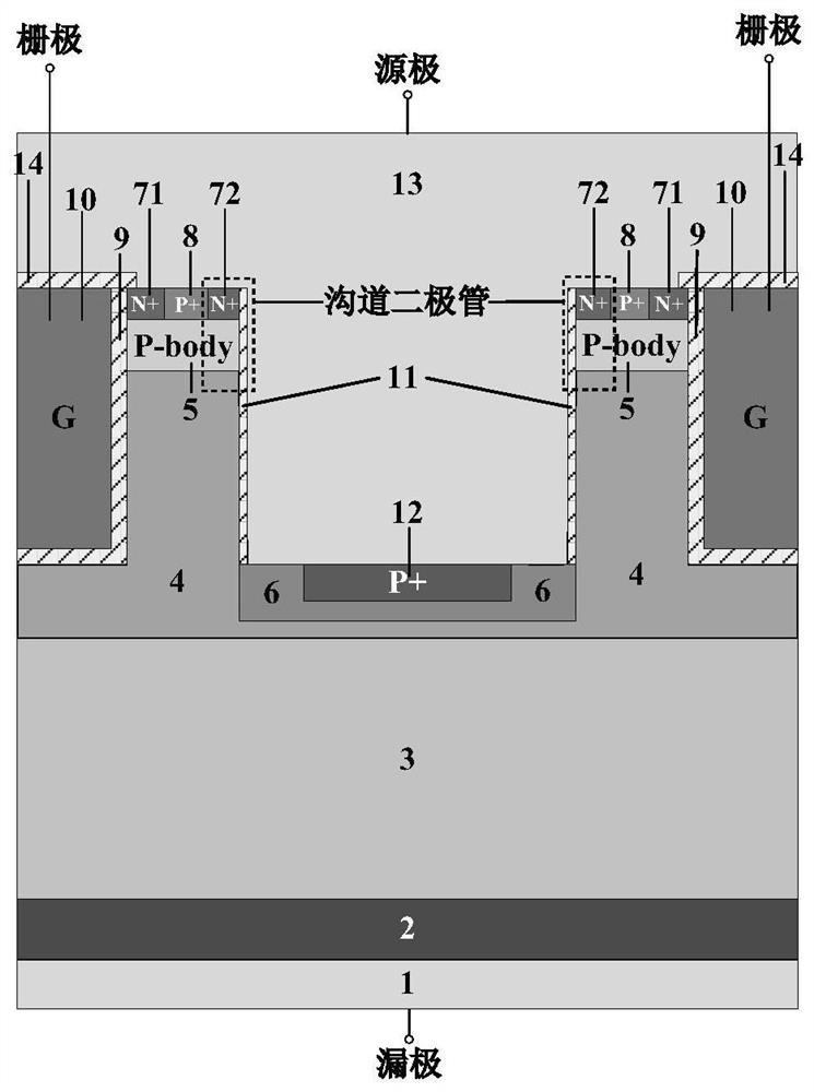
[0019] Such as figure 1 As shown, this example is

[0020] A silicon carbide double-groove MOSFET with integrated channel diodes, comprising a first conductive material 1, an N+ substrate layer 2, an N drift region 3, a JFET region 4, a P-body region 5 and a source region stacked sequentially from bottom to top structure, the source region structure is located on the upper surface of the P-body region 5;

[0021] It is characterized in that it also includes a source trench structure, the source trench structure penetrates the source region structure and the P-body region 5 along the vertical direction of the device, and then terminates in the JFET region 4, the source trench structure includes the P-region region 6, The P+ region 12 and the first insulating dielectric layer 11, the P-region region 6 is located at the lower part of the source trench, its bottom and both sides are in contact with the JFET region 4, and the P+ region 12 is embedded in the upper part of the P-reg...

Embodiment 2

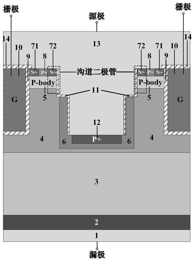
[0028] Such as figure 2 As shown, the difference between this example and Example 1 is that both ends of the P-region 6 extend upwards to form a "U"-shaped P-region, and the upper surface of the P-region 6 is flush with or lower than A stepped source trench structure is formed on the lower surface of the P-body region 5 . In the blocking state, the "U"-shaped P-region can better shield the high electric field in the oxide layer, further reduce the peak electric field in the oxide layer, and make the device have better reliability in forward blocking.


PUM


Abstract

The invention belongs to the technical field of power semiconductors, and particularly relates to a silicon carbide double-groove MOSFET (Metal-Oxide-Semiconductor Field Effect Transistor) integrated with an channel diode. The MOSFET is mainly characterized in that: firstly, a channel diode is integrated, when a device is in a follow current working mode, the channel diode is conducted to achieve a follow current function, conduction of a body diode is effectively restrained by reducing reverse conduction voltage drop, and meanwhile the influence caused by bipolar degradation is eliminated; and secondly, an electric field is modulated through a P-type region below the source groove, so that the peak of the electric field at the corner of silicon dioxide at the bottom of the gate groove is reduced, and the breakdown voltage and the reliability of the device in a blocking working mode are improved;.

Description

technical field [0001] The invention belongs to the technical field of power semiconductors, and in particular relates to a silicon carbide double-groove MOSFET with integrated channel diodes. Background technique [0002] Compared with traditional SiC planar MOS devices, SiC trench gate MOS devices have lower on-resistance due to their larger channel density and reduced influence of the JFET effect. However, SiC trench-gate MOS devices have the problem that the peak electric field of the gate oxide layer is too large. In order to solve this problem, researchers have proposed a double-slot MOSFET, which modulates the electric field through the P-type region under the source trench, so that the corner of the gate trench The peak electric field of the oxide layer is lower than the critical breakdown value, which improves the withstand voltage of the device. [0003] In converter and inverter systems, a freewheeling diode is usually required in antiparallel with the switching ...

Claims


Application Information

Patent Timeline
Patent Type & Authority Applications(China)
IPC IPC(8): H01L29/06H01L29/78H01L27/07
CPCH01L29/7827H01L29/7831H01L29/0684H01L29/0638H01L29/0623H01L27/0727Y02B70/10
Inventor 罗小蓉姜钦峰黄俊岳杨可萌马臻魏杰
Owner UNIV OF ELECTRONICS SCI & TECH OF CHINA
Why Eureka
Try Eureka