Fast recovery diode (FRD) chip and production process thereof

A technology for recovering diodes and production processes, which is applied to electrical components, semiconductor/solid-state device manufacturing, circuits, etc. It can solve problems such as unstable breakdown voltage, easy burnout of diodes, and poor anti-surge capability, and achieve enhanced withstand voltage stability performance and reliability, improve anti-surge capability, and prolong life

Active Publication Date: 2011-06-08
TIANJIN ZHONGHUAN SEMICON CO LTD
View PDF5 Cites 28 Cited by
  • Summary
  • Abstract
  • Description
  • Claims
  • Application Information

AI Technical Summary

Problems solved by technology

There are problems in the existing technology 1), the junction depth using paper source diffusion is not flat, resulting in unstable breakdown voltage and poor anti-surge capability
2), the forward voltage drop is large, resulting in large power consumption, and the diode is easy to burn out

Method used


Image

  • Fast recovery diode (FRD) chip and production process thereof
  • Fast recovery diode (FRD) chip and production process thereof
  • Fast recovery diode (FRD) chip and production process thereof

Examples


Embodiment Construction

[0026] In order to understand the present invention more clearly, describe the present invention in detail in conjunction with accompanying drawing and embodiment:

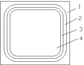
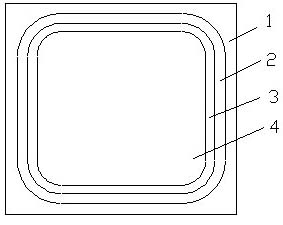
[0027] Such as figure 1 The chip structure of the fast recovery diode FRD shown is "P + NN + . Chip sections are FRD chip 1, mesa groove 2, glass layer 3, and metal surface 4 in sequence.

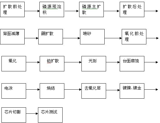
[0028] Such as figure 2 The chip process flow of the shown fast recovery diode FRD is as follows:

[0029] 1) Pre-diffusion treatment: chemically treat the surface of the silicon wafer through acid, alkali, deionized water ultrasonic cleaning and other processes.

[0030] 2) Phosphorus source pre-deposition: pre-deposit the cleaned silicon wafers in a diffusion furnace at a temperature of 1100-1200 °C by passing gas into a liquid phosphorus source.

[0031] 3) Main diffusion of phosphorus source: Diffusion advance is carried out on the pre-deposited silicon wafer in a diffusion furnace at 1200-1250 °C.

[0032] 4) P...


PUM


Abstract

The invention relates to a fast recovery diode (FRD) chip and a production process thereof. A diode with a P+NN+ structure is produced by adopting the process steps of diffusion pretreatment, double diffusion of a liquid source, back thinning, oxidization, platinum diffusion, photoetching, mesa etching, electrophoresis, sintering, scribing and the like. In the chip production process, a method of carrying out deep junction diffusion by carrying a liquid phosphorous source is adopted, so that the flatness of a diffusion junction is improved and the homogeneity and the stability of a breakdown voltage are strengthened; a method of reducing the concentration of a boron diffusion source and improving the purity of the boron diffusion source is adopted, so that the surge resistance capacity of an FRD is improved; and an electrophoresis glassivation process is adopted, so that the voltage withstanding stability and reliability of a bidirectional voltage stabilizing diode are improved. In addition, the production process has the advantages that the reverse recovery time is shortened, the switching speed is improved, the voltage drop is reduced, the power consumption is reduced, the voltage withstanding stability is improved, and the reliability of the diode is improved.

Description

technical field [0001] The present invention relates to the technical field of crystal diode chip production, in particular to a fast recovery diode (FRD) chip and its production process, carrying phosphorus liquid source diffusion, platinum diffusion, and electrophoretic glass passivation steps to make the structure P + NN + The performance of diode products is improved. Background technique [0002] At present, the production of fast recovery diode (FRD) chips in the semiconductor industry usually adopts the double diffusion production process of paper source. There are problems in the prior art 1), the junction depth of diffusion using paper source is uneven, resulting in unstable breakdown voltage and poor anti-surge capability. 2) The forward voltage drop is large, resulting in large power consumption, and the diode is easy to burn out. Contents of the invention [0003] The purpose of the present invention is exactly to overcome the deficiencies in the prior art,...

Claims


Application Information

Patent Timeline
Patent Type & Authority Applications(China)
IPC IPC(8): H01L29/861H01L21/22H01L21/329H01L21/306
Inventor 初亚东刘长蔚王军明梁效峰牛宝钢薄勇崔俊发邵枫
Owner TIANJIN ZHONGHUAN SEMICON CO LTD
Why Eureka
Try Eureka