
Method for increasing length of effective channel of PMOS

A technology of channel length and area, applied in the direction of electrical components, semiconductor/solid-state device manufacturing, circuits, etc., to increase the effective communication length of PMOS and benefit the cost

Active Publication Date: 2010-04-21
SHANGHAI HUAHONG GRACE SEMICON MFG CORP
View PDF4 Cites 2 Cited by
  • Summary
  • Abstract
  • Description
  • Claims
  • Application Information

AI Technical Summary

Problems solved by technology

[0007] The technical problem to be solved by the present invention is to provide a method to solve the problem of short channel effect in PMOS

Method used


Image

  • Method for increasing length of effective channel of PMOS
  • Method for increasing length of effective channel of PMOS
  • Method for increasing length of effective channel of PMOS

Examples


Embodiment Construction

[0021] The present invention will be further described in detail below in conjunction with the accompanying drawings and specific embodiments.

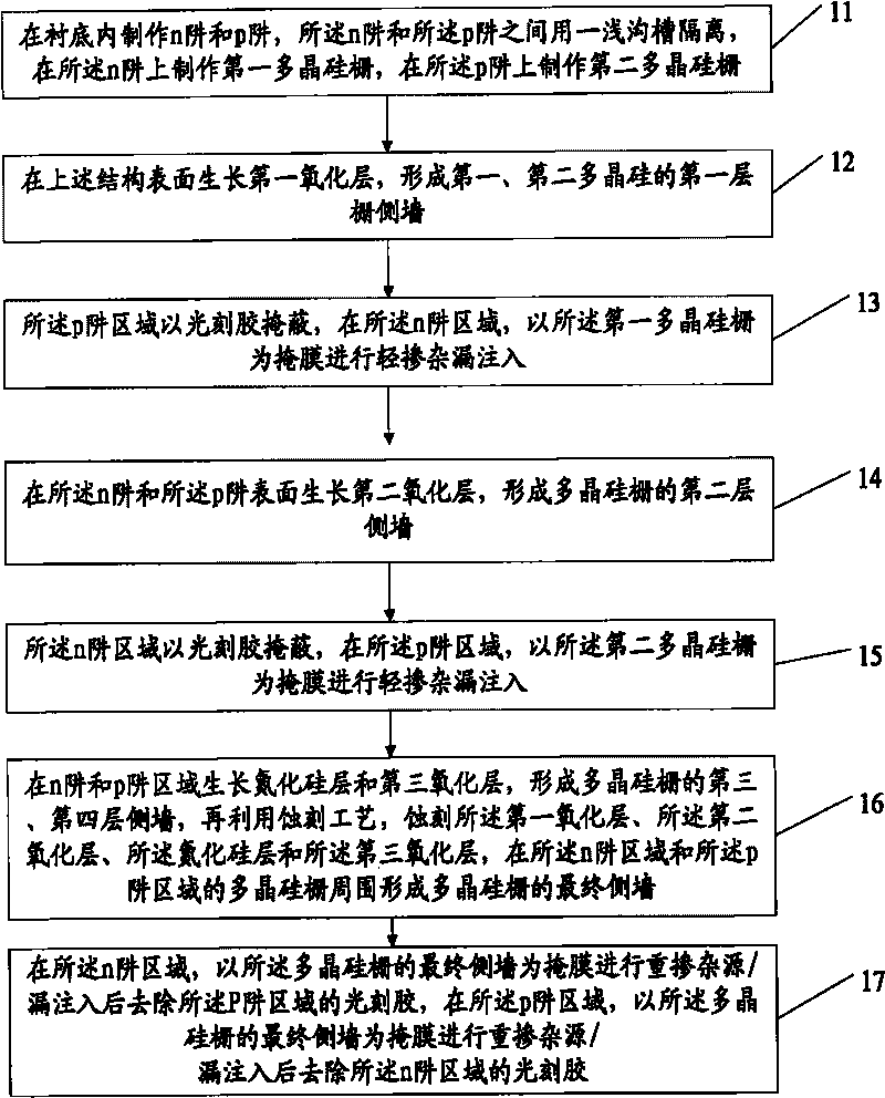
[0022] Please refer to image 3 , image 3 It is a schematic flow chart of a method for increasing the PMOS effective channel length of the present invention, comprising the following steps:

[0023] Step 11: fabricating n well and p well in the substrate, using a shallow trench isolation between the n well and the p well, fabricating a first polysilicon gate on the n well, and forming a first polysilicon gate on the p well Fabrication of the second polysilicon gate shallow trench isolation on the well is mainly divided into three steps, namely trench etching, oxide filling and oxide planarization. The fabrication of the gate structure in the transistor is the most critical step in the process, because It includes the thermal growth of the thinnest gate oxide layer and the imprinting and etching of the polysilicon gate. The basic pr...


PUM


Abstract

The invention provides a method for increasing the length of an effective channel of a PMOS, which comprises the following steps of: making an n-well and a p-well in a substrate; making a first polysilicon gate on the n-well and making a second polysilicon gate on the p-well; growing a first oxidation layer; injecting lightly doped source / drain in an n-well area; respectively growing a second oxidation layer on the surface of the n-well and the p-well; injecting lightly doped source / drain in a p-well area; respectively growing a silicon nitride layer and a third oxidation layer in the n-well and the p-well areas; etching the first oxidation layer, the second oxidation layer, the silicon nitride layer and the third oxidation layer; respectively forming a side wall around the polysilicon gates of the n-well and the p-well; injecting heavily doped source / drain in the n-well area; and injecting heavily doped source / drain in the p-well area. The method moves the step of injecting the lightly doped source / drain in the p-well area between the step of growing the second oxidation layer and the step of growing the silicon nitride layer and increases the length of the effective channel of the PMOS by using the second oxidation layer.

Description

technical field [0001] The invention belongs to a semiconductor process, in particular to a method for increasing the effective channel length of PMOS. Background technique [0002] At nodes below the 90nm process, due to the reduction of the gate feature size (for example, 65nm), severe short channel effects are caused, and the leakage current of the device increases sharply. The short-channel effect is that the threshold voltage of the MOSFET decreases as the channel length decreases. If an operating voltage is applied to the drain, the short channel effect will be exacerbated. The result of the short channel effect is to increase the leakage current of the device. In the CMOS VLSI process, the channel length will vary due to the process. Therefore, short-channel effects are a very important consideration in device design. We have to make sure that the threshold voltage of the smallest channel size in a chip is not too low. [0003] When the voltage applied to the sou...

Claims


Application Information

Patent Timeline
Patent Type & Authority Applications(China)
IPC IPC(8): H01L21/8238H01L21/336H01L21/265
Inventor 肖海波孔蔚然
Owner SHANGHAI HUAHONG GRACE SEMICON MFG CORP
Learn More