Flash memory program inhibit scheme

a flash memory and programming scheme technology, applied in the field of non-volatile memory, can solve the problems of limiting the selection to non-volatile forms of memory, affecting the performance of flash memory programs, and insufficient vpass to initiate f-n tunneling on unselected cells, etc., to achieve the effect of minimizing the disturbance of the pass

Active Publication Date: 2009-03-31
MOSAID TECH
View PDF20 Cites 32 Cited by
  • Summary
  • Abstract
  • Description
  • Claims
  • Application Information

AI Technical Summary

Benefits of technology

[0023]It is an object of the present invention to obviate or mitigate at least one disadvantage of previous Flash memory program disturb inhibit schemes. In particular, it is an object of the present invention to provide a NAND Flash memory program disturb inhibit scheme that minimizes pass disturbance of unselected memory cells during random programming operations.
[0024]In a first aspect, the present invention provides a method for minimizing program disturb in NAND string. The NAND string includes a selected memory cell, upper memory cells between the selected memory cell and a bitline, and lower memory cells between the selected memory cell and a sourceline, and a string select transistor for coupling the memory cells to the bitline. The method includes the steps of coupling a voltage level to the NAND string; precharging a channel under the selected memory cell and the upper memory cells; and locally boosting the selected memory cell channel. The voltage level corresponds to program inhibit data from the bitline. The channel under the selected memory cell and the upper memory cells are precharged to a primary boosted voltage level after the voltage level is coupled to the channel of the NAND string. The selected memory cell channel is locally boosted to a secondary boosted voltage level after the channel is precharged, the secondary boosted voltage level being higher than the primary boosted voltage level.
[0025]According to an embodiment of the aspect, the voltage level corresponding to program inhibit data is coupled to the bitline in a first time period, the channel is precharged in a second time period following the first time period, the selected memory cell channel is locally boosted in a third time period following the second time period, and the step of locally boosting includes driving a selected wordline connected to the selected memory cell to a programming voltage level. In an aspect of the present embodiment, the step of coupling can include driving the string select transistor to a first voltage level in the first time period, followed by driving the string select transistor to a decoupling voltage level in the second time period. The decoupling voltage level can be lower than the first voltage level. In another aspect of the present embodiment, the step of precharging can include driving the selected wordline cell and upper wordlines connected to the upper memory cells to a first pass voltage level. The first pass voltage can have a value effective for minimizing program disturb in the upper memory cells and for maximizing the primary boosted voltage level. The first pass voltage can be less than 10 volts, but a 7 volt pass voltage can be used.
[0026]In a further aspect of the present embodiment, wherein the step of locally boosting includes electrically turning off the upper memory cell adjacent to the selected memory cell. The step of electrically turning off can include reducing the upper wordline adjacent to the selected wordline from the first pass voltage level to a decoupling voltage level while the selected wordline is driven to the programming voltage level. Alternately, the selected wordline can be driven to the programming voltage level after the upper memory cell adjacent to the selected memory cell is turned off. More specifically, the selected wordline can be driven to the programming voltage at a delay time after the upper wordline begins to drop towards the decoupling voltage. Alternately, the step of electrically turning off can include raising the upper wordlines except the upper wordline adjacent to the selected wordline, from the first pass voltage level to a second pass voltage while the selected wordline is driven to the programming voltage level, and the upper wordline adjacent to the selected wordline can be maintained at the first pass voltage level.
[0028]In a second aspect, the present invention provides a method for minimizing program disturb in a Flash memory NAND string. The NAND string can have a selected memory cell, upper memory cells between the selected memory cell and a bitline, lower memory cells between the selected memory cell and a source line, and a string select transistor for coupling the memory cells to the bitline. The method includes a) driving the string select transistor for coupling data voltage of the bitline to the NAND string in a first time period; b) driving the upper memory cells and the selected memory cell with a pass voltage level in a second time period; c) driving the selected memory cell to a program voltage level in a third time period; and d) electrically turning off the upper memory cell adjacent to the selected memory cell in the third time period.

Problems solved by technology

In PDA's, mass storage is required for storing applications and data, while portable music players and digital cameras require large amounts of mass storage for retaining music file data and / or image data.
This limits the selection to non-volatile forms of memory since volatile memories, such as static random access memory (SRAM) and dynamic random access memory (DRAM), require a constant application of power in order to retain data.
As a result, there is a potential that erased memory cells will have their threshold voltages unintentionally shifted.
At the same time, VPASS should be insufficiently high to initiate F-N tunneling on unselected cells.
There are some problems with the basic inhibit scheme.
This leads to a drastic increase in the power consumption and the chip size, which are both highly undesirable.
High voltage transistors are larger than regular voltage transistors, which increase the page buffer size and consequently, the chip size.
However, program disturb can still occur.
In particular, if VPASS is set to be too high, erased cells coupled to BL0 can be unintentionally soft programmed to the logic “0” state due to the relatively high difference in voltage between VPASS and the 0V channel.
On the other hand, if VPASS is set to be too low, the erased memory cell connected to WL27 and coupled to BL1 may not receive sufficient channel boosting to inhibit F-N tunneling.
Unfortunately, with continued scaling down due to advances in semiconductor fabrication technology, the power supply VCC is also scaled to a lower level.
This is disadvantageous for the self-boosted inhibit scheme.
This is very problematic as the shifted thresholds can affect read operations.
Unfortunately, no random page program operations can be executed, since programmed memory cells (having Vth higher than VPASS for example) between the selected memory cell and the bitline contact will impede the bitline voltage from reaching the selected memory cell.
This random page program prohibition causes many restrictions and performance degradation in certain applications.

Method used


Image

  • Flash memory program inhibit scheme
  • Flash memory program inhibit scheme
  • Flash memory program inhibit scheme

Examples


Embodiment Construction

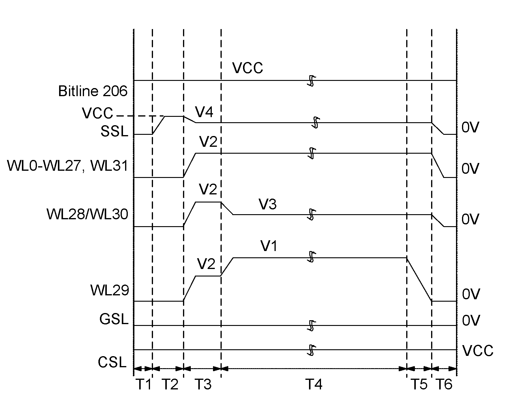
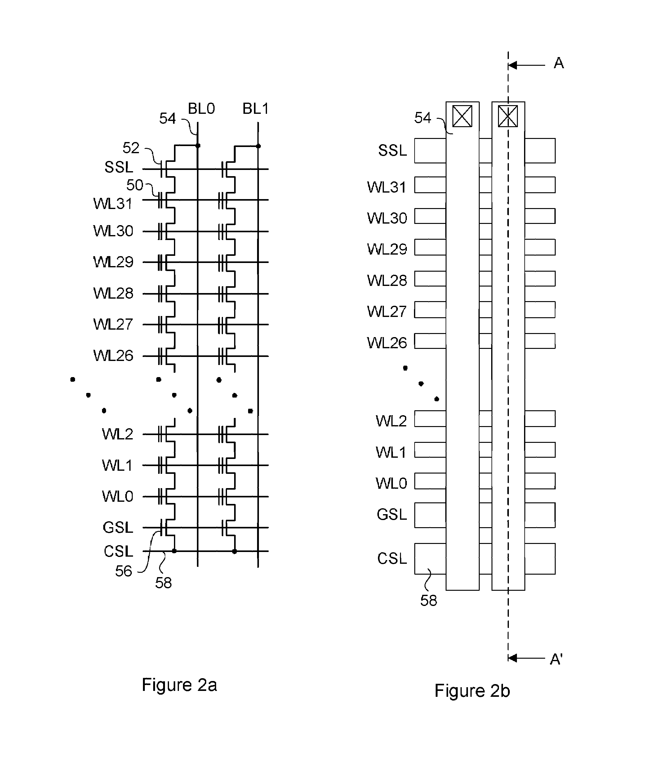
[0052]Generally, the present invention provides a method and system for minimizing program disturb in Flash memories. To reduce program disturb in a NAND Flash memory cell string where no programming from the erased state is desired, a local boosted channel inhibit scheme is used. In the local boosted channel inhibit scheme, the selected memory cell in a NAND string where no programming is desired, is locally decoupled from the other cells in the NAND string. This allows the channel of the decoupled cell to be locally boosted to a voltage level sufficient for inhibiting F-N tunneling when the corresponding wordline is raised to a programming voltage. Due to the high boosting efficiency, the pass voltage applied to the gates of the remaining memory cells in the NAND string can be reduced relative to prior art schemes, thereby minimizing program disturb while allowing for random page programming.

[0053]FIG. 5 is a flow chart illustrating a general program inhibit method according to an...


PUM


Abstract

A method for minimizing program disturb in Flash memories. To reduce program disturb in a NAND Flash memory cell string where no programming from the erased state is desired, a local boosted channel inhibit scheme is used. In the local boosted channel inhibit scheme, the selected memory cell in a NAND string where no programming is desired, is decoupled from the other cells in the NAND string. This allows the channel of the decoupled cell to be locally boosted to a voltage level sufficient for inhibiting F-N tunneling when the corresponding wordline is raised to a programming voltage. Due to the high boosting efficiency, the pass voltage applied to the gates of the remaining memory cells in the NAND string can be reduced relative to prior art schemes, thereby minimizing program disturb while allowing for random page programming.

Description

FIELD OF THE INVENTION[0001]The present invention relates generally to non-volatile memory. In particular, the present invention relates to non-volatile Flash memory programming schemes.BACKGROUND OF THE INVENTION[0002]Numerous types of consumer electronics products rely on some form of mass storage for retaining data or software for the execution of code by a microcontroller. Such consumer electronics are prolific, and include devices such as personal digital assistants (PDA's), portable music players, portable multimedia players (PMP's) and digital cameras. In PDA's, mass storage is required for storing applications and data, while portable music players and digital cameras require large amounts of mass storage for retaining music file data and / or image data. The mass storage solution for such portable electronics is preferably small in size, consumes minimal power, and has high storage density. This limits the selection to non-volatile forms of memory since volatile memories, suc...

Claims


Application Information

Patent Timeline
Patent Type & Authority Patents(United States)
IPC IPC(8): G11C16/04
CPCG11C16/0483G11C16/10G11C16/3427G11C16/3418G11C16/24G11C16/30
Inventor KIM, JIN-KI
Owner MOSAID TECH
Why Eureka
Try Eureka