Method and apparatus for designing integrated circuit enabling the yield of integrated circuit to be improved by considering random errors

a technology of random errors and integrated circuits, applied in the direction of cad circuit design, program control, instruments, etc., can solve the problems of reducing the yield of lsis manufactured, small contaminants (defects), and increasing the risk of contamination

Inactive Publication Date: 2009-03-31
FUJITSU LTD
View PDF27 Cites 198 Cited by
  • Summary
  • Abstract
  • Description
  • Claims
  • Application Information

AI Technical Summary

Benefits of technology

[0009]It is an object of the present invention to provide a layout method that enables the yield of LSIs to be improved by considering random errors in a layout design.
[0010]It is another object of the present invention to provide a layout apparatus that enables the yield of LSIs to be improved by considering random errors in a layout design.
[0011]It is yet another object of the present invention to provide a layout program that enables the yield of LSIs to be improved by considering random errors in a layout design.

Problems solved by technology

As manufacturing processes of LSIs (semiconductor integrated circuit devices) have become finer, a decrease in the yield of LSIs caused by random errors has become a more serious problem.
The random error results from “small contaminants (defects)” in a manufacturing process and shorts or opens wiring on a chip.
The random error and system errors attributed to a defect in a manufacturing process are two major factors reducing the yield of LSIs manufactured.
Thus, the layout design of LSIs or its optimization has not been carried out taking the random error as the cost of the layout design into consideration.
The random error is not considered in the layout design because it is caused by defects, so that where and how a random error occurs on a chip cannot be predicted.
Thus, the random error in the layout design is not considered.

Method used


Image

  • Method and apparatus for designing integrated circuit enabling the yield of integrated circuit to be improved by considering random errors
  • Method and apparatus for designing integrated circuit enabling the yield of integrated circuit to be improved by considering random errors
  • Method and apparatus for designing integrated circuit enabling the yield of integrated circuit to be improved by considering random errors

Examples


Embodiment Construction

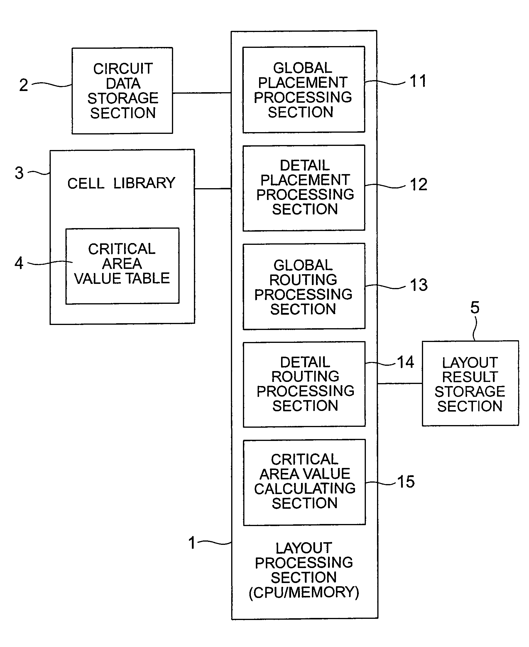
[0042]FIG. 1 is a diagram of the configuration of a layout apparatus, schematically showing the configuration of a layout apparatus that executes a layout method according to the present invention.

[0043]The layout apparatus comprises a layout processing section 1, a circuit data storage section 2, a cell library 3, a critical area value table 4, and a layout result storage section 5. In this example, the critical area value table 4 is provided in the cell library 3 as a part of it. However, the present invention is not limited to this. The layout processing section 1 comprises a global placement processing section 11, a detail placement processing section 12, a global routing processing section 13, a detail routing processing section 14, and a critical area value calculating section 15.

[0044]The circuit data storage section 2 stores, for example, circuit data obtained as a result of the design of an LSI circuit. The circuit data is not limited to those on LSIs but may be those on, f...


PUM


Abstract

A layout method in a layout apparatus for layout of an integrated circuit includes placing a plurality of cells at approximate positions according to the circuit data and placing the plurality of cells at specific positions according to the result of the placement of the plurality of cells at the approximate positions. In the placing the plurality of cells at specific positions, the plurality of cells are placed at specific positions, critical area values between cells adjacent to one another are calculated, and the specific positions of the cells are modified so as to reduce the critical area values obtained.

Description

CROSS-REFERENCE TO RELATED APPLICATIONS[0001]This is a continuation application of PCT / JP02 / 10522 filed on Oct. 10, 2002 in Japan the contents of which are incorporated herein.BACKGROUND OF THE INVENTION[0002]1. Field of the Invention[0003]This invention relates to a layout method, a layout apparatus, a layout program and a recording medium thereof, and more particularly to a layout method and a layout apparatus which enable the yield of LSIs to be improved by considering random errors in layout design, as well as a layout program and a recording medium thereof.[0004]2. Description of the Related Art[0005]As manufacturing processes of LSIs (semiconductor integrated circuit devices) have become finer, a decrease in the yield of LSIs caused by random errors has become a more serious problem. The random error results from “small contaminants (defects)” in a manufacturing process and shorts or opens wiring on a chip. The random error and system errors attributed to a defect in a manufac...

Claims


Application Information

Patent Timeline
Patent Type & Authority Patents(United States)
IPC IPC(8): G06F17/50G06F9/45
CPCG06F17/5068G06F17/5072G06F30/39G06F30/392
Inventor SHIBUYA, TOSHIYUKI
Owner FUJITSU LTD
Why Eureka
Try Eureka