Structured integrated circuit device

a technology of integrated circuits and circuit devices, applied in the direction of pulse techniques, instruments, computation using denominational number representation, etc., can solve the problems of limited configuration options, rams, roms and processors, and logical functions

Inactive Publication Date: 2009-04-07
TAHOE RES LTD
View PDF13 Cites 217 Cited by
  • Summary
  • Abstract
  • Description
  • Claims
  • Application Information

AI Technical Summary

Problems solved by technology

The advantages of such application-specific integrated circuits (ASICs) have been clearly defined in the prior art, but are limited to logical functions.
This is acceptable for Standard Cell technology, which also requires a full set of masks for the rest of the design, but can pose a problem for Structured ASIC parts, which do not.
In general RAMs, ROMs and processors, if available on FPGAs, have limited configuration options, which consist of reprogramming the interconnects between appropriate subfunctions.
This is costly in both space and performance of the components.

Method used


Image

  • Structured integrated circuit device
  • Structured integrated circuit device
  • Structured integrated circuit device

Examples


Embodiment Construction

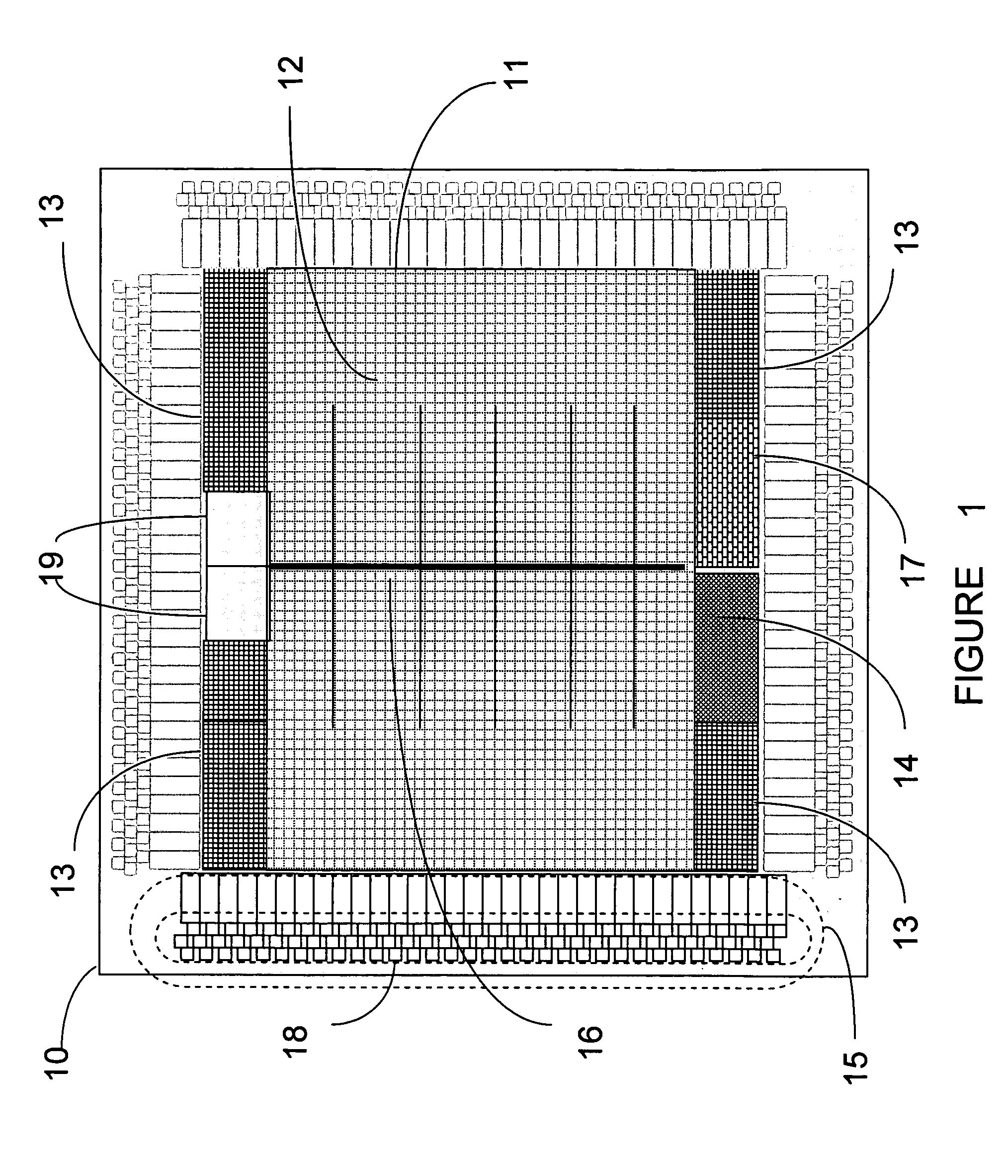
[0098]Reference is now made to FIG. 1, which is a simplified illustration of a personalizable and programmable integrated circuit device constructed and operative in accordance with a preferred embodiment of the present invention. The integrated circuit device 10 of FIG. 1 consists of a logic array 11 comprised of a multiplicity of logic cells 12 with metal connection layers, a multiplicity of configurable RAM blocks 13, a configurable ROM block 14, clock phase lock loops 19, which drive a configurable clock distribution structure 16, a built-in microprocessor 17 and a multiplicity of configurable I / O cells 15, each with associated I / O pads 18. It is further contemplated that a varying number and size of such devices may reside on many such semiconductor devices.

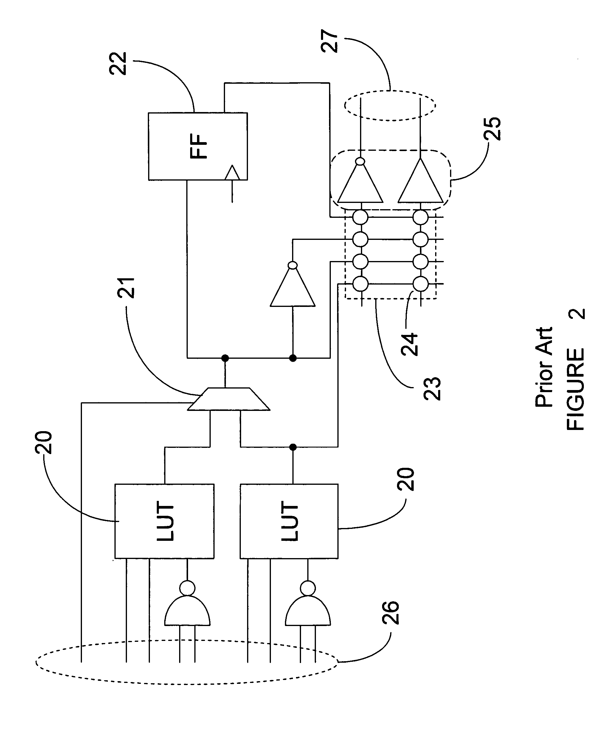
[0099]Reference is now made to FIG. 2, which is a more detailed illustration of a logic cell, as previously described in U.S. Pat. No. 6,642,744 to Or-Bach et al. The logic cells are preferably comprised of two look-up-table...


PUM


Abstract

A configurable logic array may include: a multiplicity of logic cells, containing look-up tables; customizable metal and via connection layers overlying the multiplicity of logic cells; a multiplicity of device customizable I / O cells; a multiplicity of configuration customizable RAM blocks; a ROM block with customizable contents; and a microprocessor with customizable I / O for configuring and testing the array, where the customizations are all done on a single via layer.

Description

CROSS-REFERENCE TO RELATED APPLICATIONS[0001]This application is a continuation-in-part of U.S. patent application Ser. No. 11 / 186,923, entitled “Structured Integrated Circuit Device,” filed on Jul. 22, 2005, now U.S. Pat. No. 7,157,937 which is a continuation-in-part of U.S. patent application Ser. No. 10 / 899,020, entitled “Structured Integrated Circuit Device,” filed on Jul. 27, 2004, now U.S. Pat. No. 7,098,691 both of which are commonly assigned and incorporated herein by reference.FIELD OF THE INVENTION[0002]The present invention relates to integrated circuit devices as well as to methods for personalizing, programming and testing such devices.BACKGROUND OF THE INVENTION[0003]The following U.S. patents are believed to represent the current state of the art: U.S. Pat. Nos. 6,331,733, 6,245,634, 6,236,229, and 6,194,912. These patents all relate to prior art with respect to the current patent.[0004]The above patents describe semiconductor devices, which contain logic cells that f...

Claims


Application Information

Patent Timeline
Patent Type & Authority Patents(United States)
IPC IPC(8): G06F7/38H03K19/177
CPCH03K19/17728H03K19/17732H03K19/17736H03K19/1776H03K19/17796H03K19/173
Inventor OR-BACH, ZVIWURMAN, ZE'EVLEVINTHAL, ADAM
Owner TAHOE RES LTD
Why Eureka
Try Eureka