Probe needle protection method for high current probe testing of power devices

a protection method and probe technology, applied in the direction of electrical testing, measurement devices, instruments, etc., can solve the problems of removing the power from the probe before the chip or the probe card is damaged, and achieve the effect of high curren

Active Publication Date: 2009-04-21
INTEGRATED TECH
View PDF17 Cites 14 Cited by
  • Summary
  • Abstract
  • Description
  • Claims
  • Application Information

AI Technical Summary

Benefits of technology

[0015]A method and system are provided to allow high current testing of power semiconductor chips or integrated circuit chips in wafer or chip form while limiting the maximum current of each individual probe to a safe value. Further, a method and system are provided for sensing when the contacts to the power semiconductor chip or integrated circuit chip under test are not adequate for the current levels and removing the power from the probes before the chip or the probe card is damaged. Additionally, a method and system are provided to sense the contact resistance of each probe during its use and predict potential problems before they occur so maintenance can be scheduled before catastrophic failure of the probe card.
[0017]According to one aspect of the invention, the test apparatus includes an inhibit circuit operatively coupled to the current sensor, wherein when the current sensor generates the signal, the inhibit circuit prevents current flow through each of the probes.

Problems solved by technology

Further, a method and system are provided for sensing when the contacts to the power semiconductor chip or integrated circuit chip under test are not adequate for the current levels and removing the power from the probes before the chip or the probe card is damaged.

Method used


Image

  • Probe needle protection method for high current probe testing of power devices
  • Probe needle protection method for high current probe testing of power devices
  • Probe needle protection method for high current probe testing of power devices

Examples


Embodiment Construction

[0056]The present invention will now be described with reference to the drawings, wherein like reference numerals are used to refer to like elements throughout.

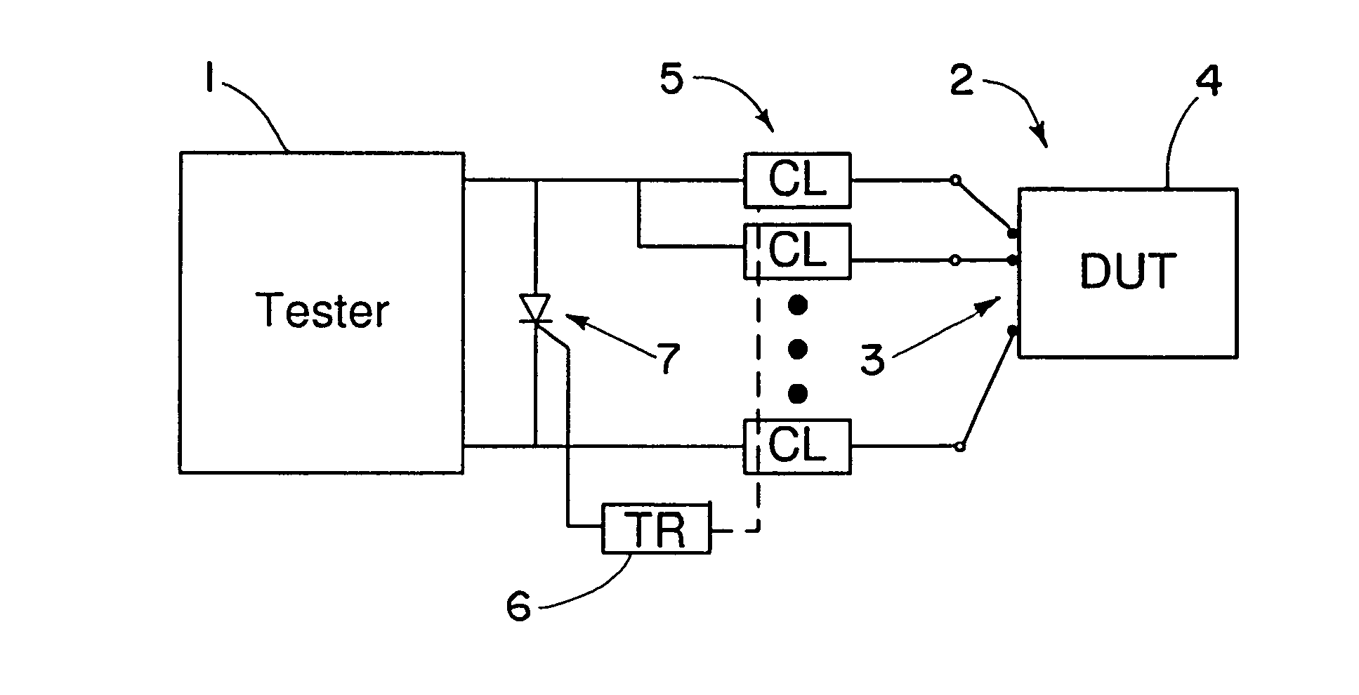
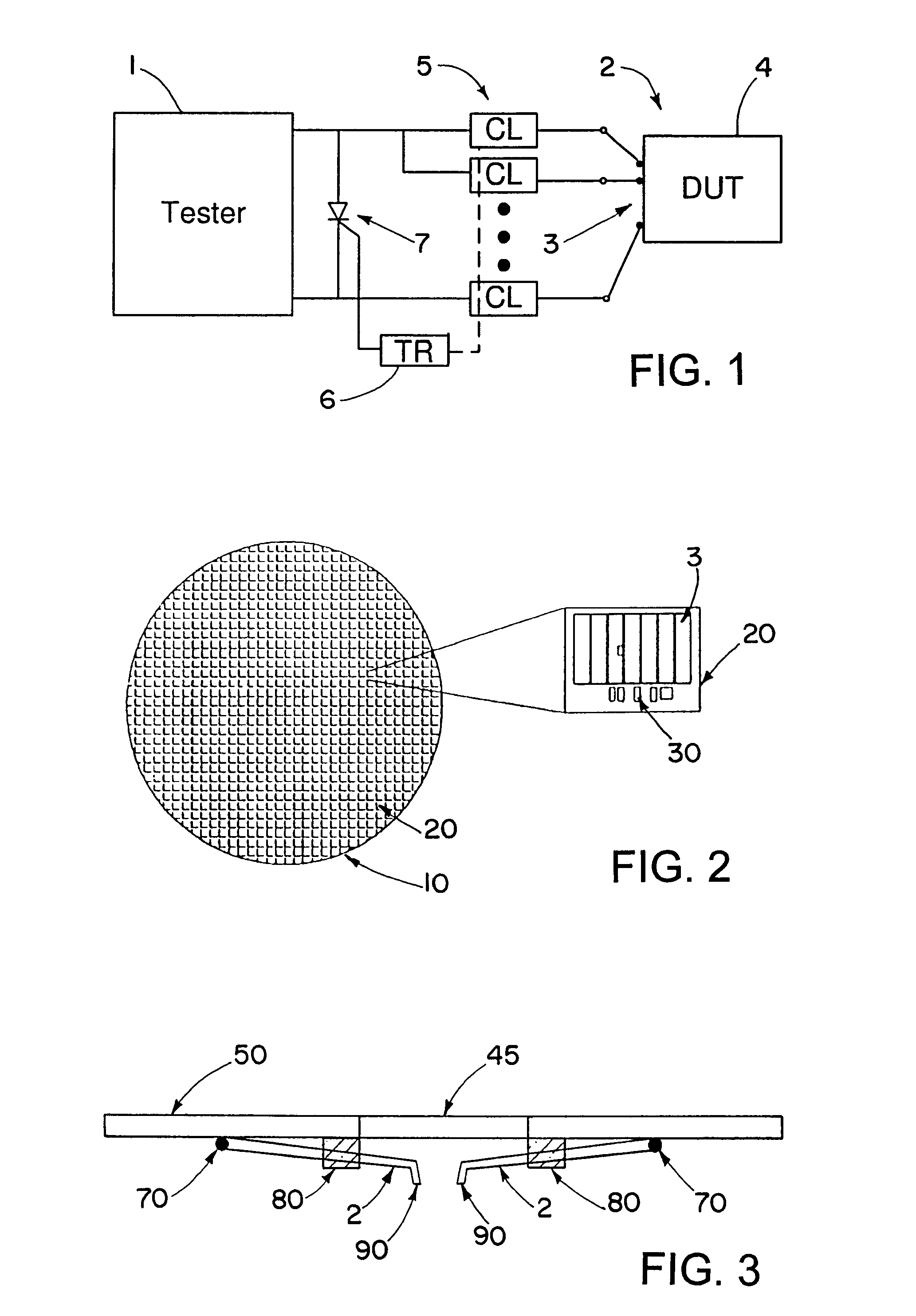
[0057]Referring initially to FIG. 1, a test apparatus 1 is shown for testing semiconductor devices while in chip or wafer form. The test apparatus 1 includes a plurality of probes 2 for contacting bonding pads 3 of a device under test 4 (DUT), e.g., a semiconductor device. A test current may be injected into the DUT 4 via the probes 2 and bonding pads 3 so as to evaluate whether or not the DUT meets certain criteria. Each probe circuit includes a current limiter 5 that is operative to limit an amount of current flowing through the respective probe 2, independent of the current flowing through other probes. By limiting current flow through the probes, damage to the probes, DUT and / or the test apparatus itself may be prevented.

[0058]Further, a trigger circuit 6 can monitor each current limiter 5 and, upon detecting certain pred...


PUM


Abstract

A test system, apparatus and method for applying high current test stimuli to a semiconductor device in wafer or chip form includes a plurality of probes for electrically coupling to respective contact points on the semiconductor device, a plurality of current limiters electrically coupled to respective ones of the plurality of probes, and a current sensor electrically coupled to the plurality of probes. The current limiters are operative to limit current flow passing through a respective probe, and the current sensor is operative to provide a signal when detected current in any contact of the plurality of probes exceeds a threshold level.

Description

RELATED APPLICATION DATA[0001]This application claims the benefit of U.S. Provisional Application No. 60 / 747,981 filed on May 23, 2006, which is incorporated herein by reference in its entirety.TECHNICAL FIELD OF THE INVENTION[0002]The present invention relates generally to the testing of semiconductor chips, such as power semiconductor chips and more particularly, to a method and apparatus for testing power semiconductor chips in wafer or chip form by making reliable contact to the chip via probing needles.BACKGROUND OF THE INVENTION[0003]Power semiconductor devices are fabricated by a series of batch processes in which wafers, typically of silicon or other compatible material, are processed to produce a particular type of power semiconductor chip. Each wafer contains a plurality of power semiconductor die or chips, typically of the same kind. As is known, chemical, thermal, photolithographic and mechanical operations are typically involved in the fabrication of the power semicondu...

Claims


Application Information

Patent Timeline
Patent Type & Authority Patents(United States)
IPC IPC(8): G01R31/02G01R1/00G01R31/26
CPCG01R1/36G01R1/06766G01R31/2886
Inventor ROGERS, GARYCLAUTER, STEVESCHWARTZ, RODNEYUKAI, TAICHILAMBRIGHT, JOELOHR, DAVE
Owner INTEGRATED TECH
Why Eureka
Try Eureka