Testing device and testing method

Active Publication Date: 2011-12-22
FUJI ELECTRIC CO LTD
View PDF10 Cites 16 Cited by
  • Summary
  • Abstract
  • Description
  • Claims
  • Application Information

AI Technical Summary

Benefits of technology

[0013]According to the testing device and testing method of the invention, it is possible to realize a high voltage testing

Problems solved by technology

There is a possibility of the device to be tested or testing device being damaged, and a possibility of the testing of the device to be tested not being carried out correctly.
However, a gas with a high insulation property, typified by sulfur hexafluoride gas, has a high global warming potential (GWP), and the burden on the global environment is large.
However, with the method whereby an insulation shield is disposed in the discharge p

Method used


Image

  • Testing device and testing method
  • Testing device and testing method
  • Testing device and testing method

Examples


Example

First Embodiment

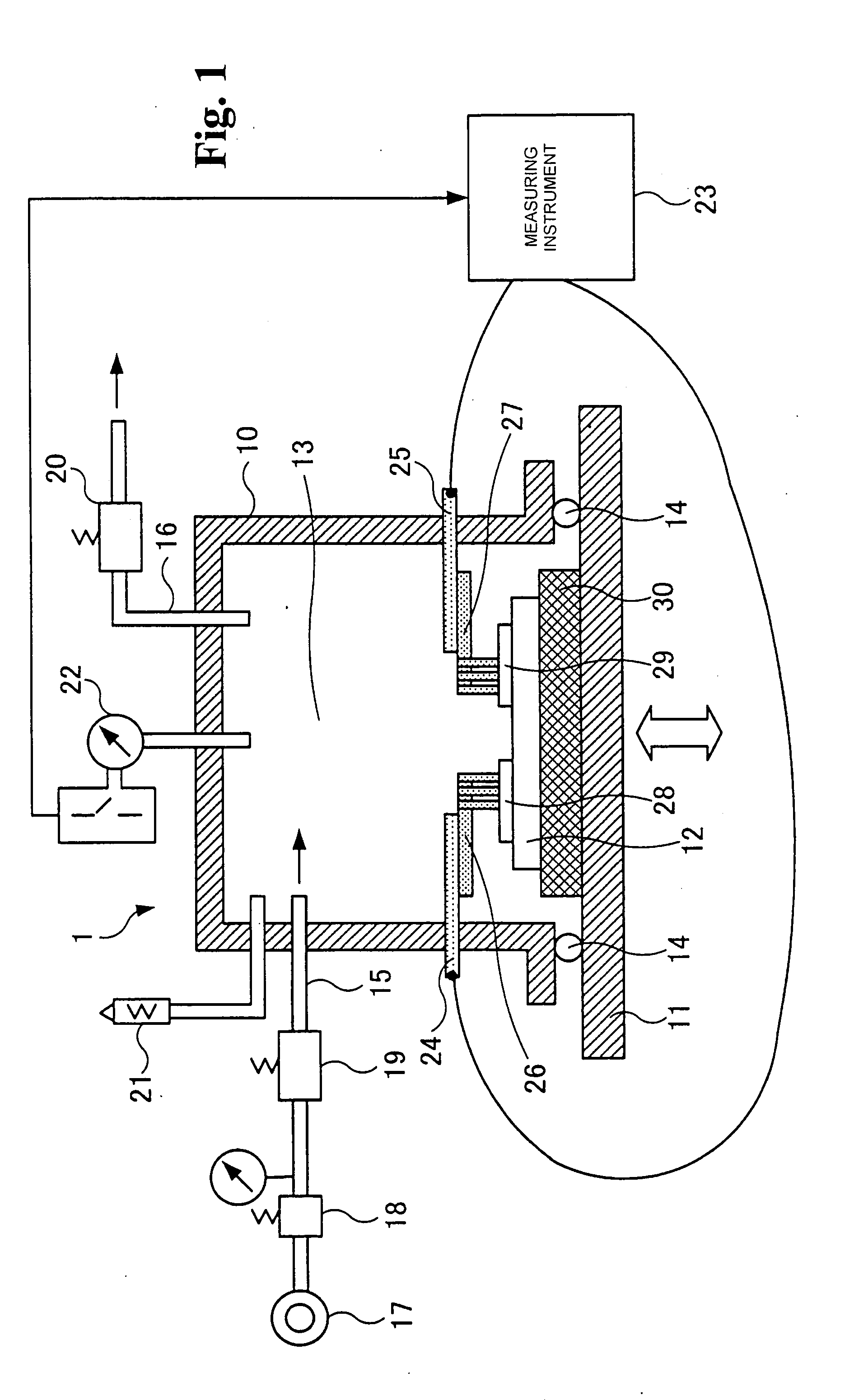
[0033]FIG. 1 is a diagram showing one example of a testing device according to a first embodiment.

[0034]A testing device 1 has a pressure vessel 10, a bottom plate 11, and a measuring instrument 23. The pressure vessel 10 has an internal space 13 in which testing of a device to be tested (DUT) 12 is carried out, and can withstand pressure until the pressure of the internal space 13 reaches a specified pressure. The pressure vessel 10 may also be called, for example, a chamber. Herein, an example is given of a case in which the device to be tested 12 is a semiconductor device including electrodes 28 and 29. Also, the device to be tested 12 may be any one of a semiconductor wafer, a semiconductor chip, a semiconductor package, or a semiconductor module. The testing device 1 may be a wafer prober, a handler, or the like, as appropriate in accordance with the devices 12 to be tested.

[0035]The bottom plate 11 is disposed in such a way as to cover the internal space 13 of ...

Example

[0076]Next, a description will be given, as a second embodiment, of an embodiment using a pressurization unit other than that of the testing device 1 for raising the atmospheric pressure of the internal space 13 of the pressure vessel 10.

Second Embodiment

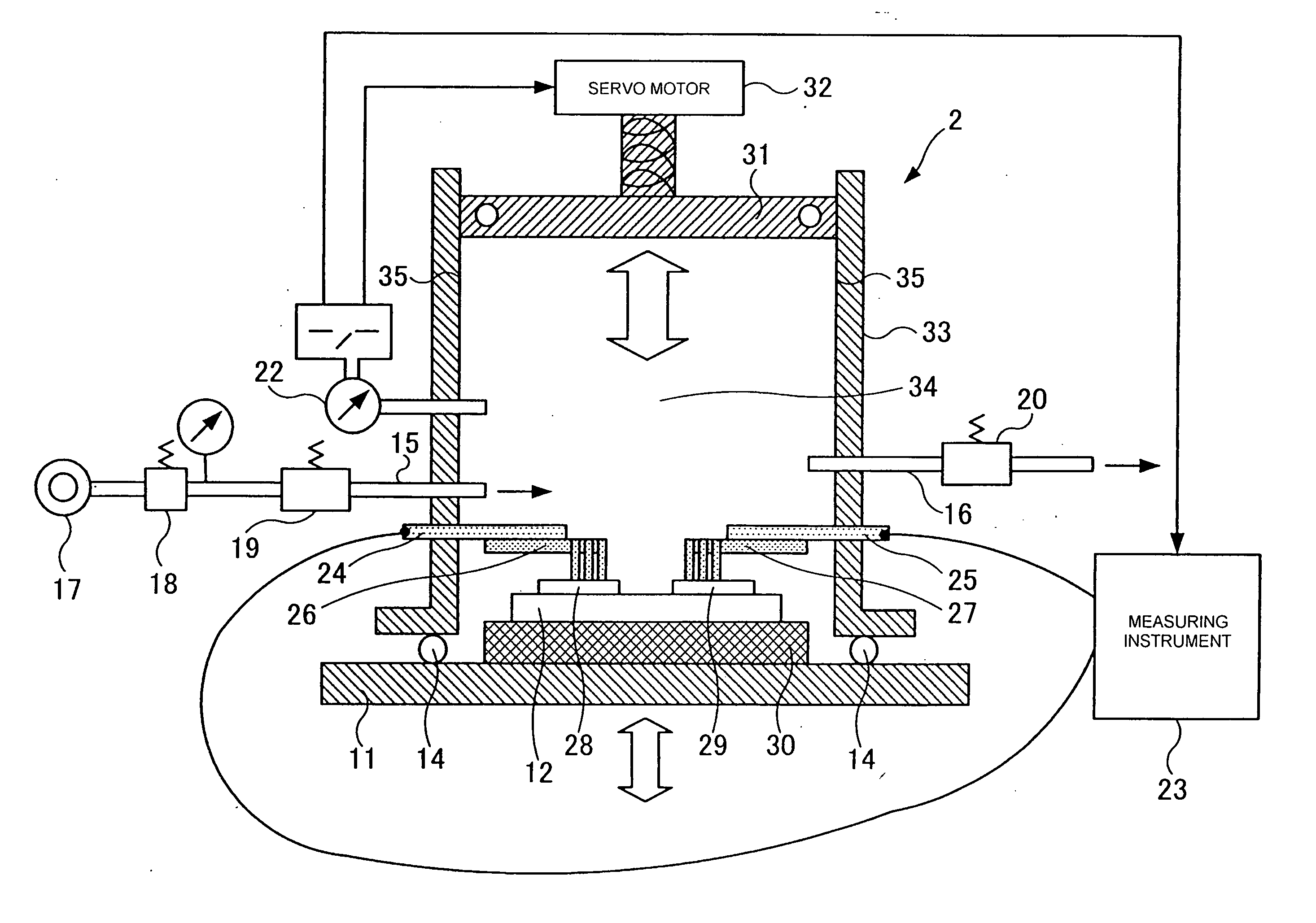
[0077]FIG. 4 is a diagram showing one example of a testing device according to the second embodiment.

[0078]A testing device 2 is such that the form of a pressure vessel differs in comparison with that of the testing device 1, and furthermore, a piston 31 and a servomotor 32 are additionally provided. Also, although no relief valve is provided, one may be provided. Other configurations are the same as those of the testing device 1.

[0079]A pressure vessel 33 has an aperture at the top thereof. The piston 31 is disposed in such a way as to block the aperture of the pressure vessel 33. The servomotor 32 is provided on the piston 31. The piston 31 raises or lowers an internal space 34 of the pressure vessel 33 by being controlled by the ...

Example

[0119]Next, a description will be given, as a third embodiment, of one example of a dielectric strength test to which the testing methods of the first and second embodiments are applied.

Third Embodiment

[0120]FIGS. 7A and 7B are diagrams showing one example of a dielectric strength test according to the third embodiment. FIG. 7A is a top view of a device 40 to be tested, and FIG. 7B is a sectional view of the device 40 to be tested to which test electrodes 47a and 47b are attached.

[0121]As shown in FIG. 7A, the device 40 to be tested has a frame electrode 41, a plurality of lead terminals 42 and 43, and a semiconductor chip 44. The semiconductor chip 44 is formed on the frame electrode 41, and the semiconductor chip 44 and lead terminals and 43 are electrically connected by internal wires 45. Furthermore, the frame electrode 41, a plurality of lead terminals 42 and 43, semiconductor chip 44, and internal wires 45 are sealed with a resin 46. Herein, an end portion of the frame electro...


PUM


Abstract

A testing device includes a pressure vessel, a mounting stand disposed in an internal space of the pressure vessel, on which a device to be tested is mounted, test electrodes, disposed in the internal space of the pressure vessel, that supply a test voltage to the device to be tested mounted on the mounting stand, and a pressurization unit that raises the pressure of the internal space of the pressure vessel. The test voltage is supplied from the test electrodes to the device to be tested mounted on the mounting stand, and testing of the device to be tested is carried out, in a condition that the pressure of the internal space of the pressure vessel is raised by the pressurization unit.

Description

BACKGROUND OF THE INVENTION AND RELATED ART STATEMENT[0001]The present invention relates to a testing device and testing method for carrying out a high voltage testing of a device to be tested.[0002]A testing method exists whereby a high voltage test is supplied to a device to be tested, and a high voltage testing of the device is carried out. With this kind of testing method, a dielectric breakdown and a discharge occurs between electrodes of the device to be tested, or between electrodes of the device to be tested and a testing device, and the like. There is a possibility of the device to be tested or testing device being damaged, and a possibility of the testing of the device to be tested not being carried out correctly.[0003]For this reason, a technology exists whereby the device to be tested is disposed in an environment of a gas with a high insulation property, for example, sulfur hexafluoride gas (SF6), and high voltage testing is performed after ensuring the dielectric stren...

Claims


Application Information

Patent Timeline
IPC IPC(8): G01R31/28
CPCG01R31/129G01R31/2881G01R31/16
Inventor YOSHIDA, ATSUSHITOYA, HIROYUKINISHIZAWA, TORUUCHIYAMA, SEIZO
Owner FUJI ELECTRIC CO LTD
Why Eureka
Try Eureka