Display with multiple emission layers

a technology of emission layer and display, applied in the field of display, can solve the problems of deteriorating the quality of displayed images, uneven brightness over the display, and the length of the service life of the display, so as to reduce the variation of brightness between pixels, accurately display gradational images, and reduce power loss

Active Publication Date: 2009-05-05
JVC KENWOOD CORP
View PDF10 Cites 22 Cited by
  • Summary
  • Abstract
  • Description
  • Claims
  • Application Information

AI Technical Summary

Benefits of technology

[0029]The present invention has been made in consideration of the problems mentioned above. An object of the present invention is to provide a display capable of greatly reducing brightness variations among pixels on a screen of the display, accurately displaying gradational images, reducing a power loss, and realizing a long service life.
[0040]The display according to the present invention can greatly reduce pixel brightness unevenness over a screen of the display, precisely display gradation levels, minimize a power loss, and elongate a service life.
[0041]The display of the present invention digitally drives the light emitting element of a dot to express a gradation level intended for the dot according to the sum of brightness weights. Namely, without the influence of variations in the threshold values of the first driver, the display can drive each light emitting element, to thereby eliminate brightness unevenness over the screen of the display and reduce a power loss.
[0042]According to the present invention, a current necessary for realizing an intended brightness level is not entirely passed to a single emission layer. Namely, the present invention distributes the current to a plurality of emission layers. This results in extending the service life of the display of the present invention compared with the related arts.
[0043]The present invention expresses a gradation level of a dot with the sum of brightness of n emission layers. This results in extending the service life of the display of the present invention compared with the conventional display that passes a current necessary for realizing a required brightness level to a single emission layer.

Problems solved by technology

This results in varying the brightness of light from pixel to pixel, to cause brightness unevenness over the display and deteriorate the quality of displayed images.
This method, however, is disadvantageous in the length of service life of a display because a current necessary for an intended brightness level is entirely passed to one emission layer to increase load on the emission layer.
In addition, the method has a flickering problem because each gradation level is achieved with emission and no-emission periods.
However, it has an interference problem of causing, for example, pseudo contours on moving images.
Hei-11-073159 and No. 2003-280593 necessitate a plurality of sub-pixels for every pixel, and therefore, are not suitable for the trend of high-resolution panels in the future.

Method used


Image

  • Display with multiple emission layers
  • Display with multiple emission layers
  • Display with multiple emission layers

Examples


first embodiment

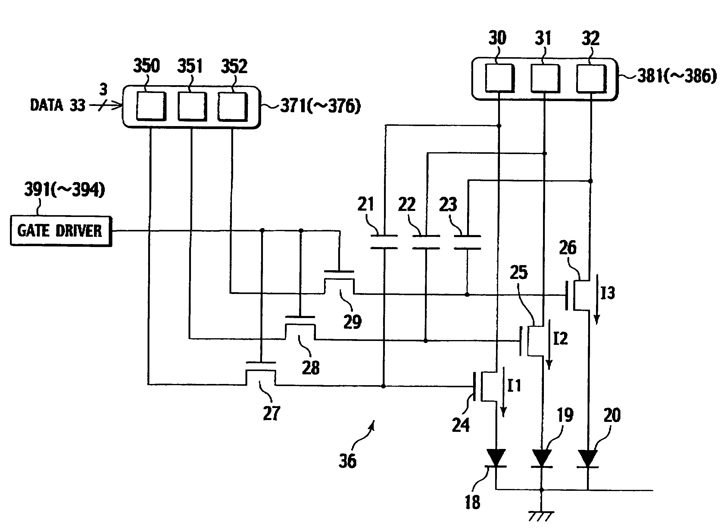
[0077]FIG. 5 shows a layer structure of a pixel in a display according to a first embodiment of the present invention. This display is, for example, an organic EL display. A glass substrate 1 is a screen of the display. The glass substrate 1 may be made of, for example, plastic material if it is useful to form organic film layers thereon. On the glass substrate 1, an anode 2 is formed. The anode 2 is, for example, a transparent ITO electrode.

[0078]On the anode 2, an organic emission layer 3 is formed. The organic emission layer 3 is a combination of a hole injection layer, a hole transport layer, an electron injection layer, an electron transport layer, and an emission layer made of organic luminescent compounds. The combination must be properly selected according to organic EL characteristics.

[0079]On the organic emission layer 3, a cathode 4 is formed. If the cathode 4 is a transparent ITO electrode, it will not operate as a cathode if used as it is. It is necessary to insert, for...

second embodiment

[0116]A pixel in a display according to a second embodiment of the present invention will be explained in detail. The first embodiment mentioned above forms the organic emission layers from different materials so that the layers may emit light of different brightness levels, i.e., may provide different brightness weights. The second embodiment forms organic emission layers from the same material and applies different current values to the layers for different periods, so that the layers may emit light of predetermined brightness levels. The second embodiment will be explained in detail with reference to first to seventh examples of brightness weighting techniques.

[0117]The layer-structure and configuration of a pixel according to the second embodiment are the same as those of the first embodiment, and therefore, the explanation thereof will be omitted. The brightness weight of each layer of the second embodiment is based on FIG. 7A, and the gradation level expression of the second e...

third embodiment

[0163]A pixel in a display according to a third embodiment of the present invention will be explained in detail. The first and second embodiments each employ a pixel composed of organic emission layers that are digitally driven. The third embodiment employs pixels each composed of emission layers that are driven in an analog mode and emission layers that are digitally driven.

[0164]FIG. 18 shows a layer structure of a pixel in the display according to the third embodiment. A glass substrate 301 is a screen of the display. The glass substrate 301 may be made of, for example, plastic material suitable for forming organic film layers thereon. On the glass substrate 301, an anode 302 is formed. The anode 302 is, for example, a transparent ITO electrode.

[0165]On the anode 302, an organic emission layer 303 is formed. The organic emission layer 303 is a combination of a hole injection layer, a hole transport layer, an electron injection layer, an electron transport layer, and an emission l...


PUM


Abstract

A display has light emitting elements, a first driver, a power source, and a second driver. Each light emitting element includes “n” emission layers formed one over another to form a color dot in each pixel. The first driver drives the emission layers to emit light or no light. The power source passes a current through the first driver to the light emitting element. The second driver individually weights the n emission layers and makes the emission layers emit light so that each dot may express a gradation level.

Description

BACKGROUND OF THE INVENTION[0001]1. Field of the Invention[0002]The present invention relates to a display, and particularly, to a display such as an electroluminescence display with a plurality of emission layers laid one over another, to display gradational images.[0003]2. Description of Related Art[0004]Organic electroluminescence displays (OELDs) are drawing attention because they are very thin and are high in contrast, response speed, and viewing angles. Hereafter, the organic electroluminescence display is sometimes referred to as “organic EL display.” The organic EL display uses organic compounds that demonstrate an electroluminescence effect to convert electricity into light. The organic EL display frequently employs an active matrix driving method to improve energy efficiency and reduce energy consumption. Due to these and other advantages, the organic EL display is regarded as a promising next-generation display.[0005]FIGS. 1A and 1B show layer structures employed for conv...

Claims


Application Information

Patent Timeline
Patent Type & Authority Patents(United States)
IPC IPC(8): G09G3/30G09G3/20G09G3/32H01L27/32H01L51/52
CPCG09G3/3233H01L51/5278G09G3/2011G09G3/2014G09G3/2022G09G3/2074G09G3/2081G09G2300/0443G09G2300/0842G09G2320/0233G09G2320/0276G09G2330/02H01L27/3209H10K59/32H10K50/19
Inventor OHSHIMA, YOSHINORIMASUJI, SHIGEHIROHIROHATA, NAOTO
Owner JVC KENWOOD CORP
Why Eureka
Try Eureka