Apparatus for translated wafer stand-in tester

a technology of stand-in testers and wafers, which is applied in the direction of electronic circuit testing, measurement devices, instruments, etc., can solve the problems of not packaging integrated circuits that cannot perform as desired, and none of these analytical or repair tools emulate closely the actual production configuration of the wafer-level test apparatus

Active Publication Date: 2009-05-12
TRANSLARITY INC
View PDF6 Cites 17 Cited by
  • Summary
  • Abstract
  • Description
  • Claims
  • Application Information

AI Technical Summary

Problems solved by technology

In this way, integrated circuits that cannot perform as desired are not packaged, or otherwise incorporated into finished products.
None of these analytical or repair tools emulate closely the actual production configuration of the wafer-level test apparatus.

Method used


Image

  • Apparatus for translated wafer stand-in tester
  • Apparatus for translated wafer stand-in tester
  • Apparatus for translated wafer stand-in tester

Examples


Embodiment Construction

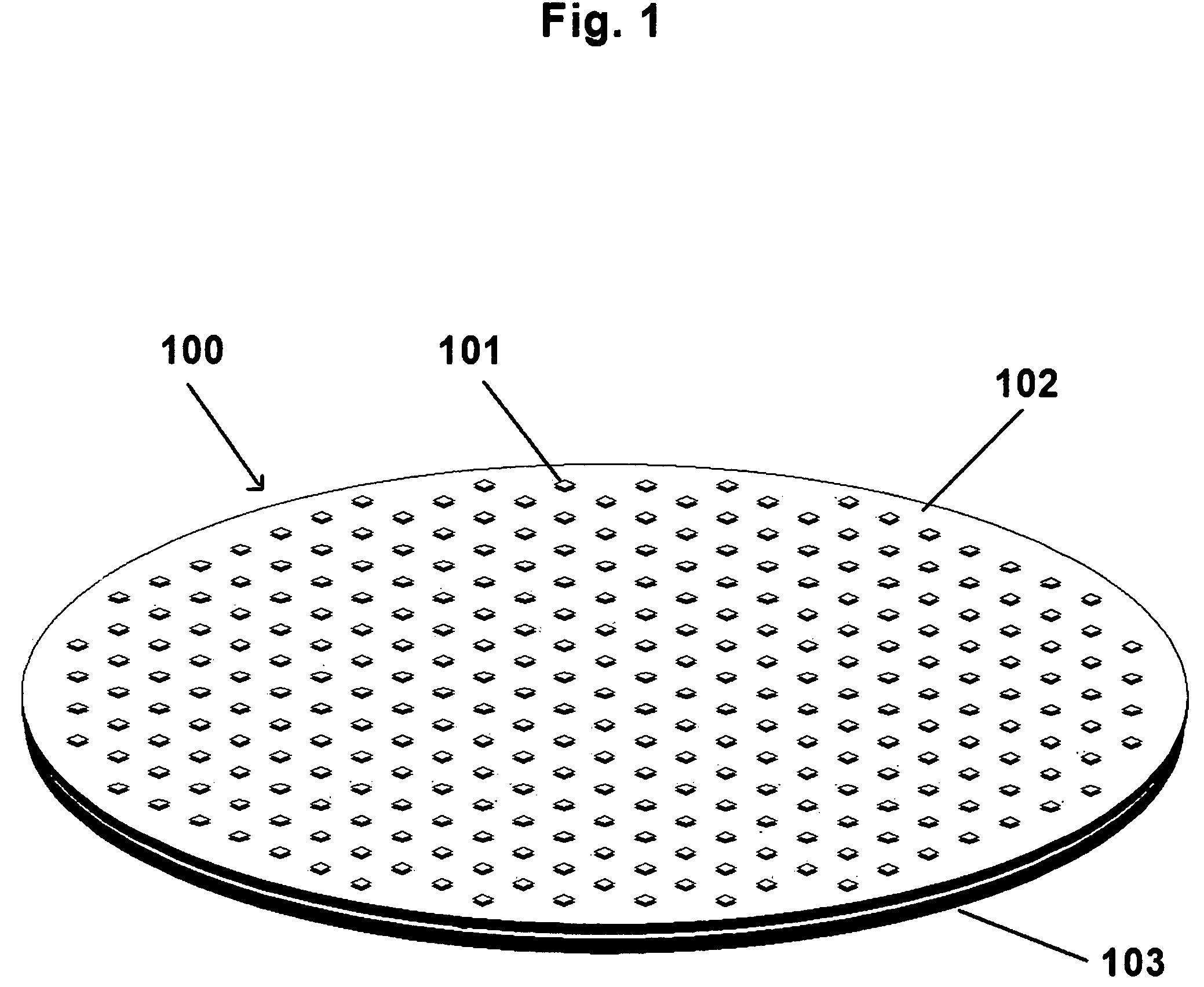
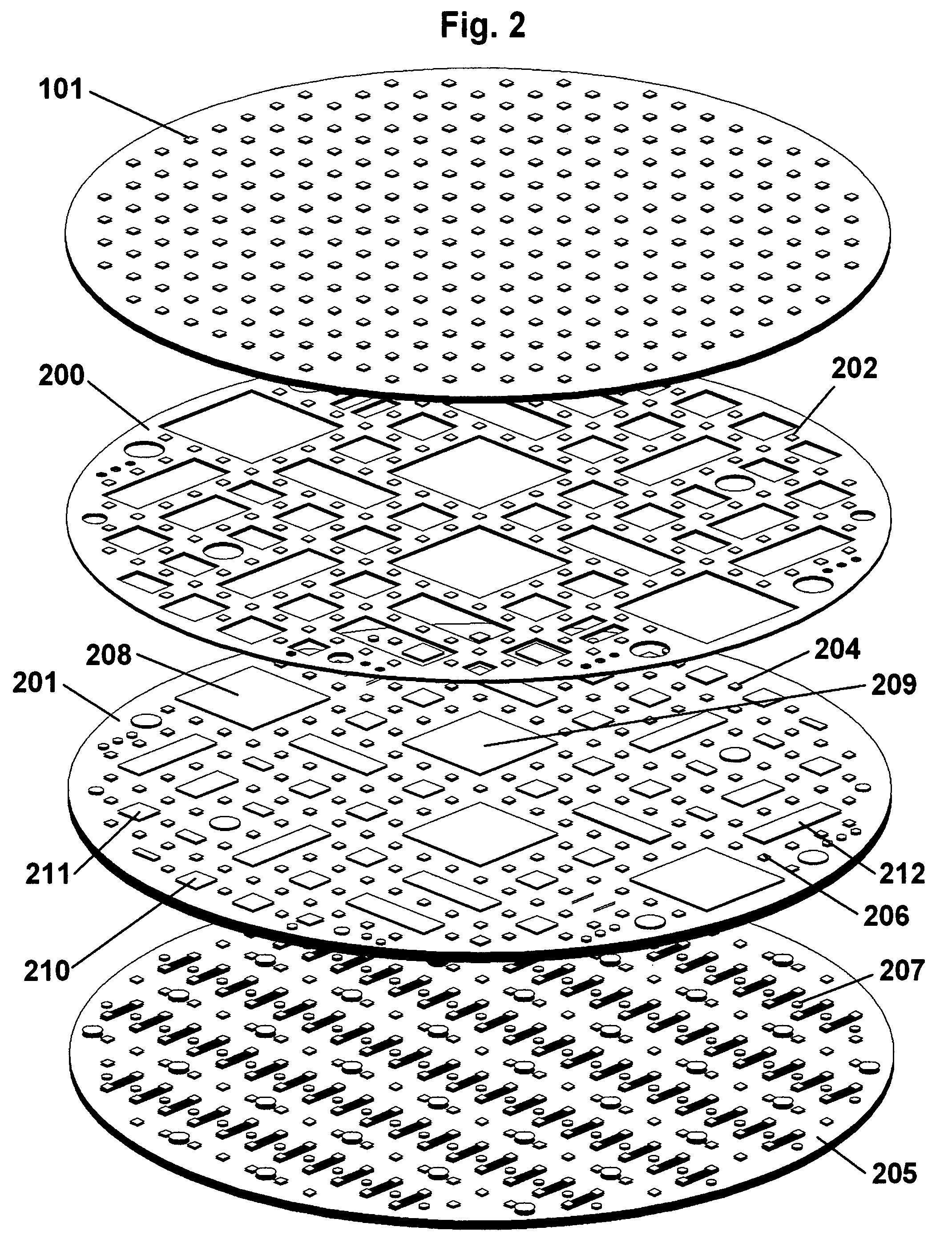
[0018]Generally, embodiments of the present invention provide an active replacement for a translated wafer, wherein this replacement may be used to characterize, or otherwise interact with, a wafer-level test system.

[0019]Reference herein to “one embodiment”, “an embodiment”, or similar formulations, means that a particular feature, structure, operation, or characteristic described in connection with the embodiment, is included in at least one embodiment of the present invention. Thus, the appearances of such phrases or formulations herein are not necessarily all referring to the same embodiment. Furthermore, various particular features, structures, operations, or characteristics may be combined in any suitable manner in one or more embodiments.

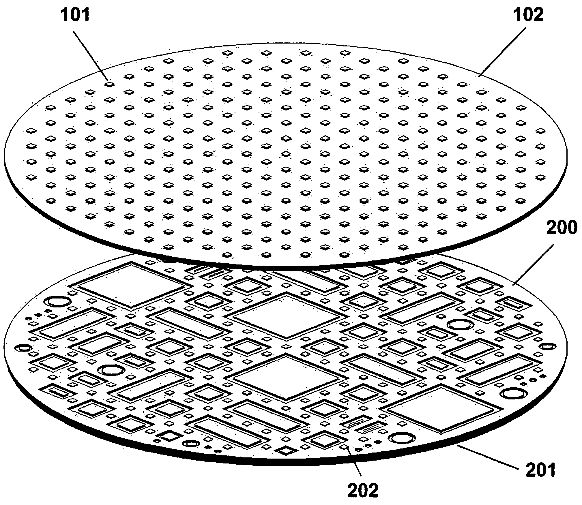
[0020]In its operational mode, a wafer-level test assembly verifies the functionality of circuits on a translated wafer. To test the functionality of the test equipment, a translated wafer stand-in tester (TWST) that emulates the form factor ...


PUM


Abstract

A translated wafer stand-in tester (TWST), being a hybrid apparatus capable of emulating the form factor and some or all behaviors of a translated wafer under test, which is operable to store, quantify, encode and convey, either directly or remotely, data from a testing system, including but not limited to pad pressure, electrical contact and temperature. The TWST may include several stacked and attached layers, at least one internal layer including electronic components operable to interact with a test system.

Description

CROSS-REFERENCE TO RELATED APPLICATIONS[0001]This non-provisional application claims the benefit of provisional applications 60 / 811,484, filed 6 Jun. 2006, and entitled “Methods and Apparatus for Translated Wafer Stand-In Tester”; 60 / 811,673 filed 6 Jun. 2006, and entitled “Methods and Apparatus for Single Wafer Stand-In Tester”; and 60 / 836,488, filed 8 Aug. 2006, and entitled “Methods and Apparatus for Monolithic Wafer Stand-in Tester”; and the entirety of each is hereby incorporated by reference.FIELD OF THE INVENTION[0002]The present invention relates generally to semiconductor test equipment, and more particularly relates to methods and apparatus for the evaluation and maintenance of a semiconductor test system.BACKGROUND[0003]Advances in semiconductor manufacturing technology have resulted in, among other things, reducing the cost of sophisticated electronics to the extent that integrated circuits have become ubiquitous in the modern environment.[0004]As is well-known, integrat...

Claims


Application Information

Patent Timeline
Patent Type & Authority Patents(United States)
IPC IPC(8): G01R31/02
CPCG01R31/286
Inventor JOHNSON, MORGAN T.
Owner TRANSLARITY INC
Why Eureka
Try Eureka