Method of fabricating an organic field transistor

a transistor and organic field technology, applied in the field of electric detection of selected species, can solve the problems of poor sensitivity, polymer conductivity, and limited practical application of such electric devices

Inactive Publication Date: 2009-05-19
ALCATEL-LUCENT USA INC
View PDF13 Cites 4 Cited by
  • Summary
  • Abstract
  • Description
  • Claims
  • Application Information

AI Technical Summary

Benefits of technology

[0017]The present invention further recognizes the advantages of forming biosensor devices having a semiconductive film that includes electrically conducting organic molecules with probe molecules attached substantially to the outer surface of the film. The complete or substantial absence of probe molecules in the interior of the film facilitates the formation of uniform closely packed crystalline or polycrystalline films of the organic molecules. This is advantageous because the charge transfer characteristics of the film depends on the efficient packing of the organic molecules, which generally have one or more conjugated Pi bonds, to form a system of conjugated Pi bonds. The efficiency of charge transfer from one organic molecule to another increases as the distance between the conjugated Pi bonding systems of adjacent organic molecules is decreased.

Problems solved by technology

The present invention recognizes that the practical application of such electric devices has been limited due to poor sensitivity, in part, because functionalizing the side-chains of the organic polymer reduces the polymer's conductivity.
Moreover, the binding of the target biomolecules to the probe molecules attached throughout the organic polymer does not result in a sufficiently large change in conductivity to allow the detection of small quantities of the target biomolecule.

Method used


Image

  • Method of fabricating an organic field transistor
  • Method of fabricating an organic field transistor
  • Method of fabricating an organic field transistor

Examples


Embodiment Construction

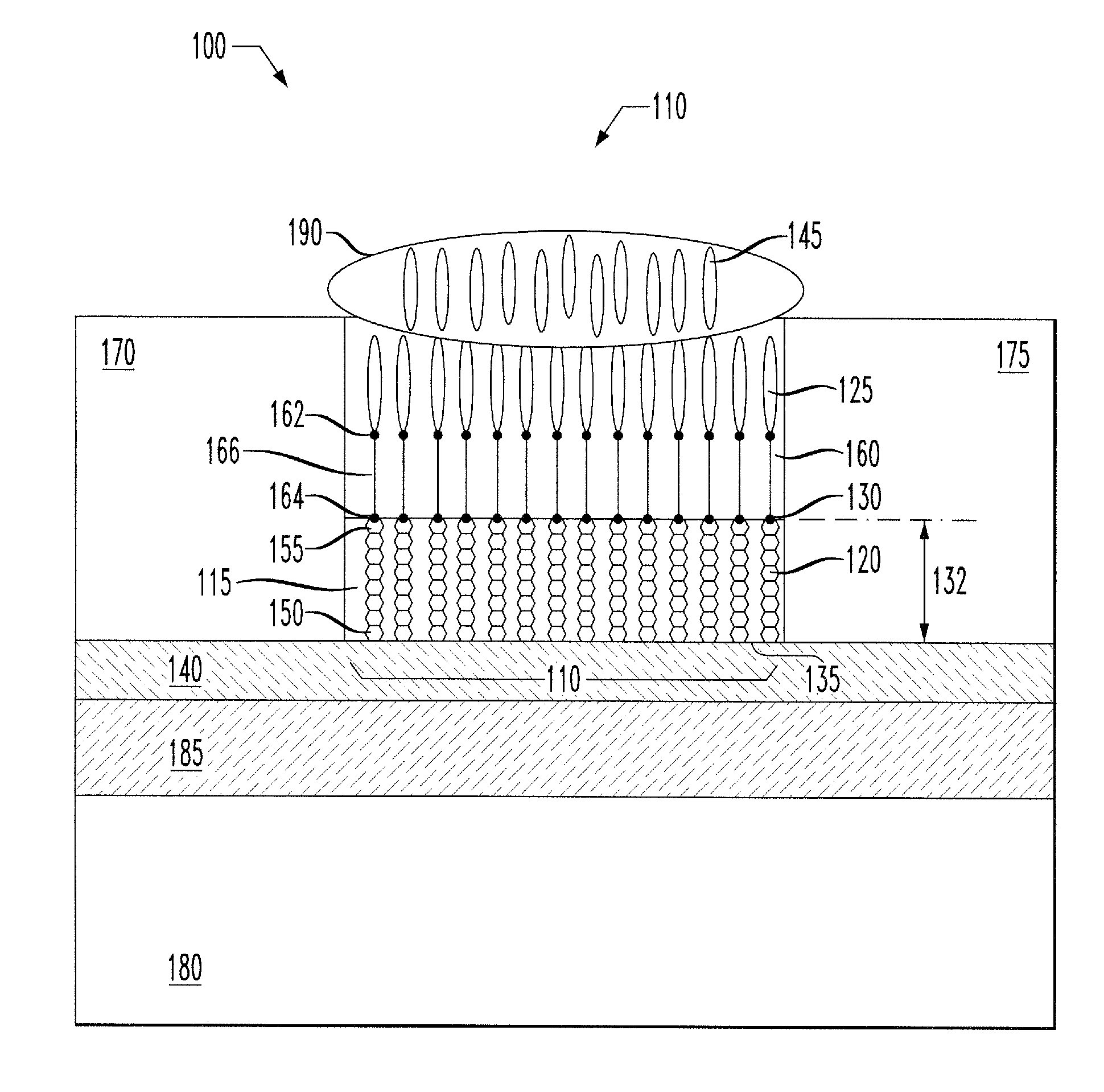
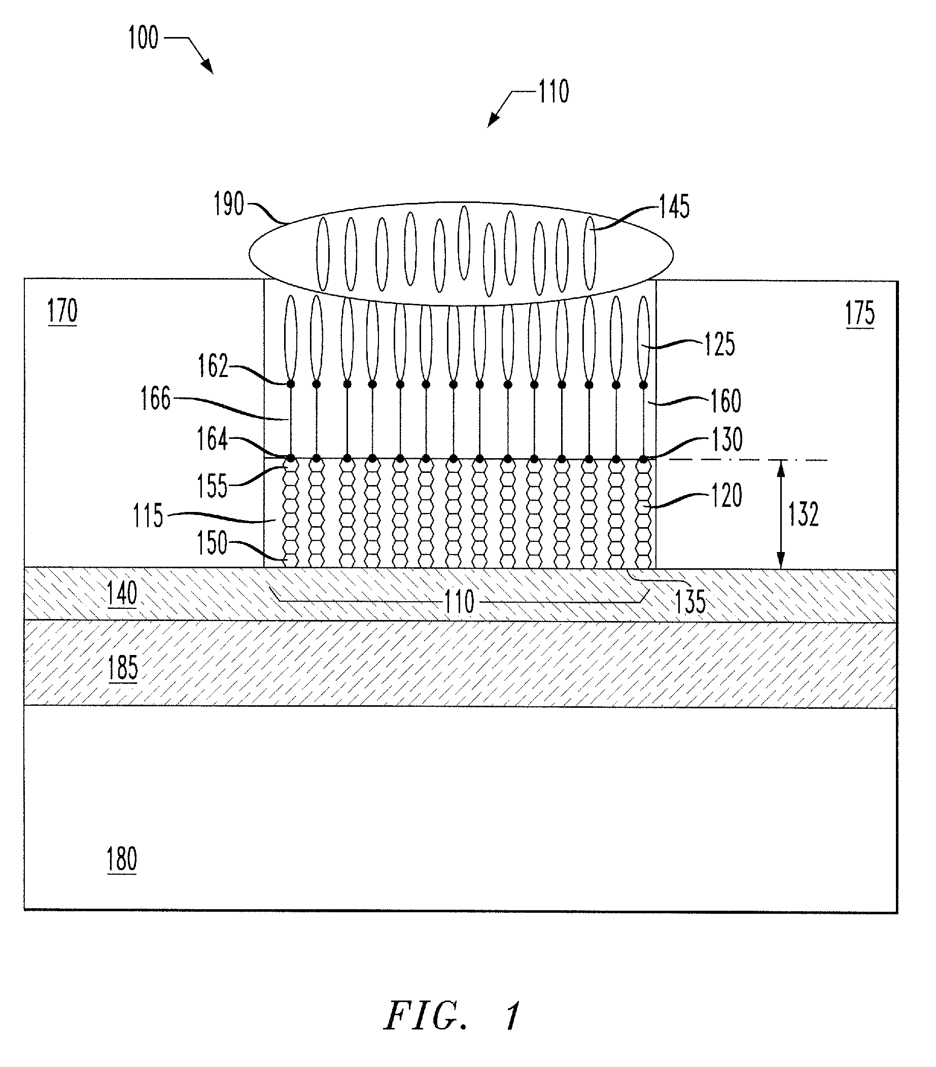
[0016]The present invention benefits from the realization that previous biosensors for detecting biological target molecules have poor conductivity because probe molecules are attached to the interior side-chains throughout the organic polymers of the semiconductive film in the biosensor. Probe molecules comprising nuclei acid or amino acid sequences, such as DNA or proteins, impede the formation of ordered semiconductive films composed of the functionalized organic polymers. This, in turn, detrimentally decreases the efficiency of charge transfer between the semiconductive organic polymers of the semiconductive film. Moreover, the present invention recognizes that probe molecules, such as DNA, have substantial insulating properties when they are incorporated throughout the interior of such films, thereby further decreasing the conductivity of the films.

[0017]The present invention further recognizes the advantages of forming biosensor devices having a semiconductive film that includ...


PUM


Abstract

The present invention provides an organic field effect transistor and a method of fabricating the transistor. The transistor includes a semiconductive film comprising organic molecules. Probe molecules capable of binding to target molecules are coupled to an outer surface of the semiconductive film such that the interior of the film being substantially free of the probe molecules.

Description

CROSS-REFERENCE TO RELATED APPLICATION[0001]This Application is a Divisional of U.S. patent application Ser. No. 10 / 405,398 entitled, “THE ELECTRICAL DETECTION OF SELECTED SPECIES,” to Zhenan Bao, et al., filed on Apr. 2, 2003 now U.S. Pat. No. 7,189,987, which is commonly assigned with the present invention and incorporated herein by reference as if reproduced herein in its entirety under Rule 1.53(b).TECHNICAL FIELD OF THE INVENTION[0002]The present invention is directed, in general, to the electrical detection of selected species, in particular biologically relevant species. More specifically, the invention is directed to a biosensor device that includes an organic field effect transistor and a method of manufacturing the device.BACKGROUND OF THE INVENTION[0003]There is great interest in the rapid simultaneous detection of large numbers of biological species such as naturally occurring DNA, RNA, proteins, and other naturally occurring molecules, as well as man-made aptamers, synt...

Claims


Application Information

Patent Timeline
Patent Type & Authority Patents(United States)
IPC IPC(8): H01L21/00C12Q1/68G01N27/414H01L21/8234H01L27/088H01L29/786H01L51/05H01L51/30H01L51/40
CPCG01N27/4145G01N27/414H10K10/462
Inventor BAO, ZHENANYURKE, BERNARD
Owner ALCATEL-LUCENT USA INC
Why Eureka
Try Eureka