Solid-state imaging element and solid-state imaging apparatus

a technology of solid-state imaging and imaging elements, which is applied in the direction of picture signal generators, television systems, radioation controlled devices, etc., can solve problems such as reducing sensitivity

Active Publication Date: 2019-08-22
SONY SEMICON SOLUTIONS CORP
View PDF3 Cites 3 Cited by
  • Summary
  • Abstract
  • Description
  • Claims
  • Application Information

AI Technical Summary

Benefits of technology

[0005]Incidentally, a solid-state imaging apparatus is desired to improve charge transfer efficiency.
[0006]It is desirable to provide a solid-state imaging element that allows for an improvement in charge transfer efficiency and a solid-state imaging apparatus including the solid-state imaging element.
[0009]In the solid-state imaging element according to the embodiment of the present disclosure and the solid-state imaging apparatus according to the embodiment of the present disclosure, of the pair of electrodes opposed to each other with the photoelectric conversion layer and the insulation layer having the first opening interposed therebetween, the one electrode provided on the side on which the insulation layer is located includes a plurality of electrodes (the first electrode and the second electrode), and the first electrode is embedded in the first opening to be electrically coupled to the photoelectric conversion layer. This allows for two-dimensional movement of charges generated in the photoelectric conversion layer by photoelectric conversion.
[0010]According to the solid-state imaging element according to the embodiment of the present disclosure and the solid-state imaging apparatus according to the embodiment of the present disclosure, of the pair of electrodes opposed to each other with the photoelectric conversion layer and the insulation layer having the first opening interposed therebetween, the one electrode provided on the side on which the insulation layer is located includes the first electrode that is embedded in the first opening provided in the insulation layer to be electrically coupled to the photoelectric conversion layer, which causes two-dimensional movement of charges in the photoelectric conversion layer. This makes it possible to improve transfer efficiency of charges retrieved from the first electrode.

Problems solved by technology

Moreover, in a case where a color filter including two-dimensionally arranged primary color filters of red, green, and blue is used for colorization, for example, green light and blue light are absorbed by the color filter in a red pixel, thereby leading to reduced sensitivity.

Method used


Image

  • Solid-state imaging element and solid-state imaging apparatus
  • Solid-state imaging element and solid-state imaging apparatus
  • Solid-state imaging element and solid-state imaging apparatus

Examples


first embodiment (

1. First Embodiment (an example in which an opening for coupling between a photoelectric conversion layer and a readout electrode is filled with the readout electrode)

1-1. Configuration of Solid-state Imaging Element

1-2. Method of Manufacturing Solid-state Imaging Element

1-3. Workings and Effects

[0048]2. Second Embodiment (an example in which a transfer electrode is provided)

third embodiment (

3. Third Embodiment (an example in which a discharging electrode is provided)

4. Modification Example (an example in which a semiconductor layer is provided between a lower electrode and a photoelectric conversion layer)

5. Application Examples

1. FIRST EMBODIMENT

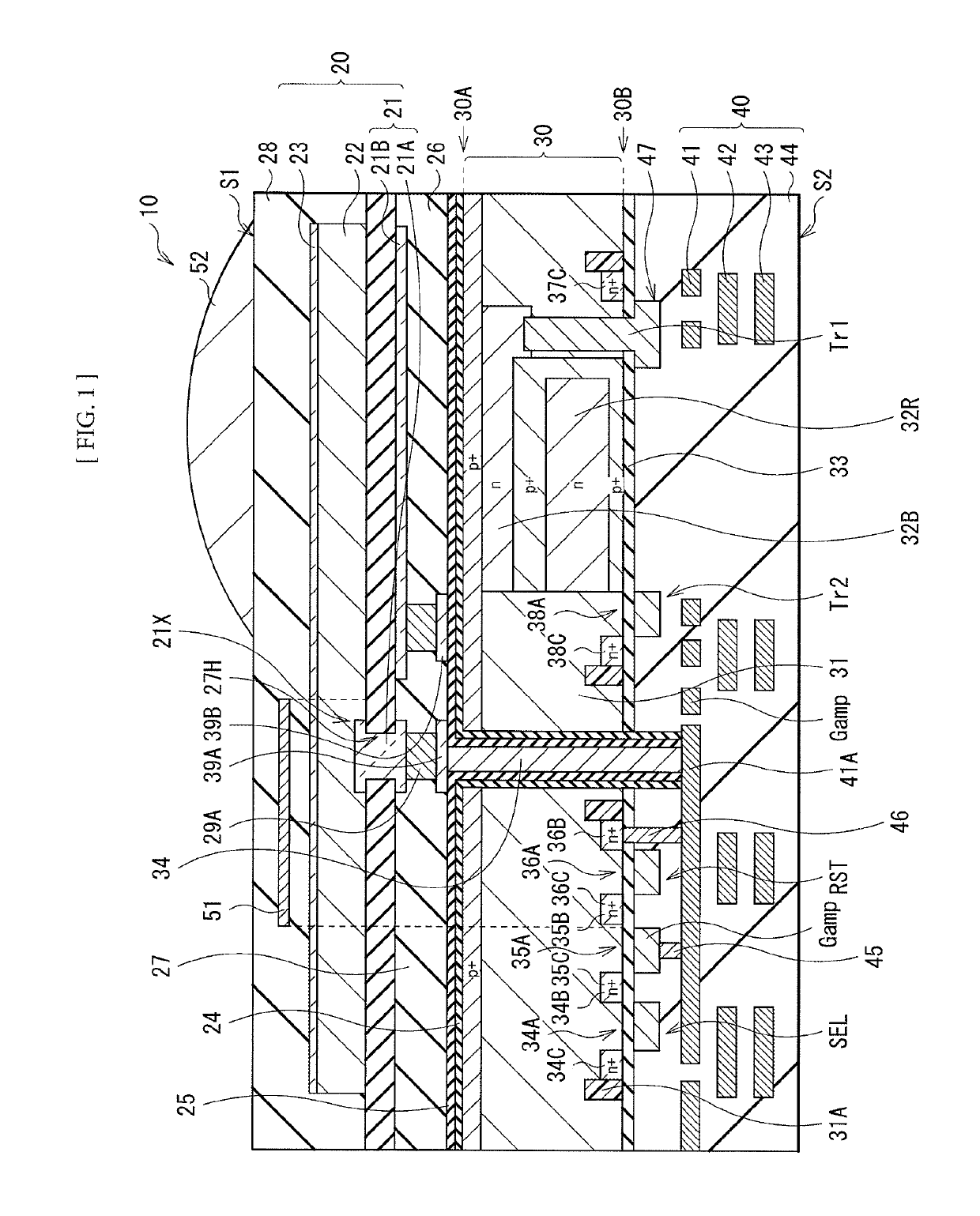
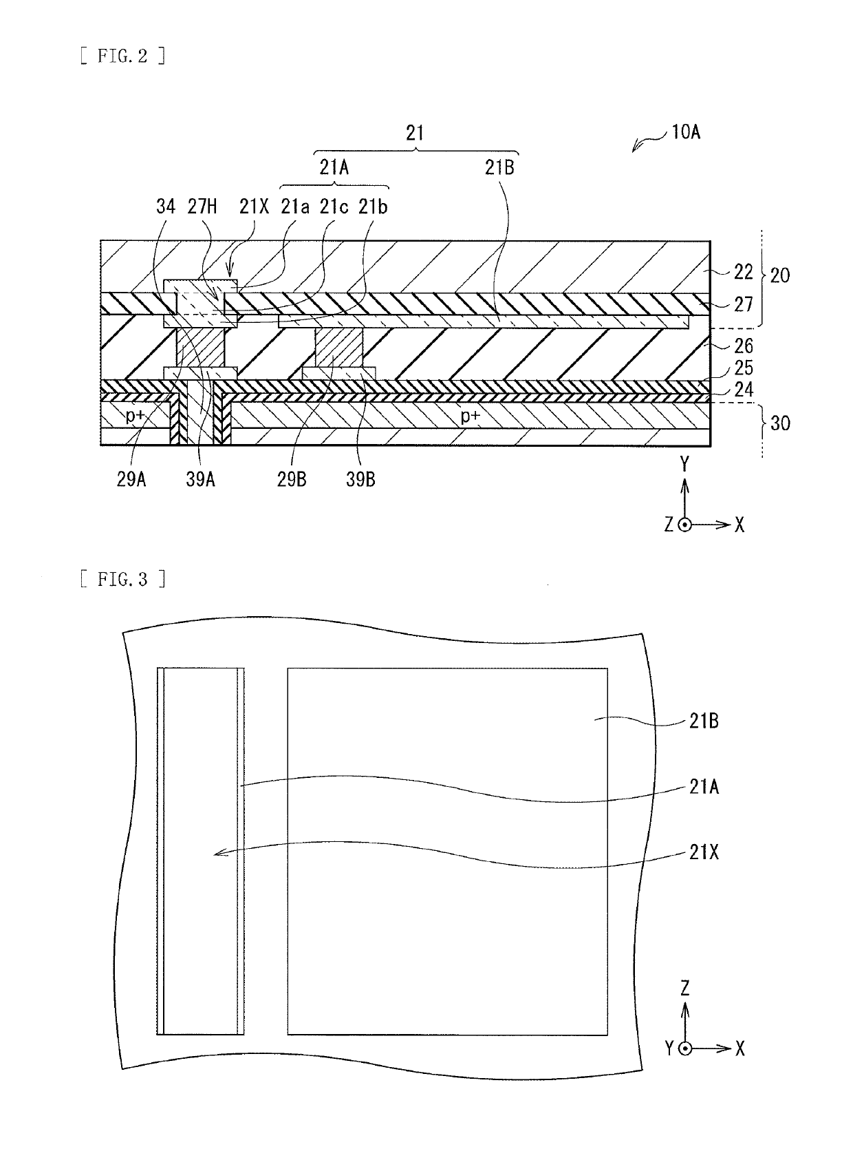
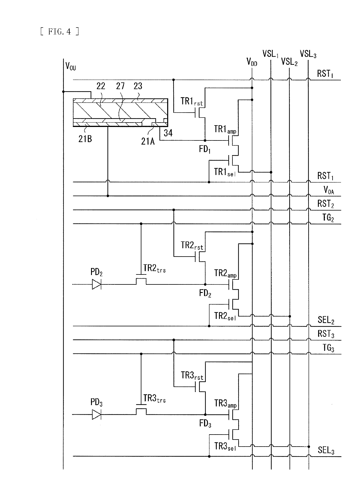
[0049]FIG. 1 illustrates a cross-sectional configuration of a solid-state imaging element (a solid-state imaging element 10A) according to a first embodiment of the present disclosure. FIG. 2 illustrates an enlarged cross-sectional configuration of a main part (an organic photoelectric converter 20 and its surroundings) of the solid-state imaging element 10A illustrated in FIG. 1. FIG. 3 schematically illustrates a planar configuration of a lower electrode illustrated in FIG. 2. FIG. 4 is an equivalent circuit diagram of the solid-state imaging element 10A illustrated in FIG. 1. FIG. 5 schematically illustrates a layout of a lower electrode 21 and transistors included in a controller in the solid-state imaging element 10A illu...

second embodiment

2. SECOND EMBODIMENT

[0129]FIG. 17 schematically illustrates a cross-sectional configuration of a main part of a solid-state imaging element (a solid-state imaging element 10B) according to the second embodiment of the present disclosure. FIG. 18 schematically illustrates a planar configuration of a lower electrode illustrated in FIG. 17. As with the foregoing first embodiment, the solid-state imaging element 10B is of a so-called longitudinal direction spectral type in which, for example, one organic photoelectric converter 60 and two inorganic photoelectric converters 32B and 32R are stacked in the longitudinal direction. The solid-state imaging element 10B according to the present embodiment differs from the foregoing first embodiment in that a lower electrode 61 included in the organic photoelectric converter 60 includes three electrodes including a readout electrode 61A, an accumulation electrode 61B, and a transfer electrode 61C.

[0130]The transfer electrode 61C improves transfe...


PUM


Abstract

A solid-state imaging element according to an embodiment of the present disclosure includes: a photoelectric conversion layer; an insulation layer provided on one surface of the photoelectric conversion layer and having a first opening; and a pair of electrodes opposed to each other with the photoelectric conversion layer and the insulation layer interposed therebetween. Of the pair of electrodes, one electrode provided on a side on which the insulation layer is located includes a first electrode and a second electrode each of which is independent, and the first electrode is embedded in the first opening provided in the insulation layer to be electrically coupled to the photoelectric conversion layer.

Description

TECHNICAL FIELD[0001]The present disclosure relates to a solid-state imaging element using, for example, an organic semiconductor material, and a solid-state imaging apparatus including the solid-state imaging element.BACKGROUND ART[0002]In recent years, in a solid-state imaging apparatus such as a CCD (Charge Coupled Device) image sensor or a CMOS (Complementary Metal Oxide Semiconductor) image sensor, miniaturization of pixel size has been under way. This causes a reduction in the number of photons entering a unit pixel, thereby resulting in reduced sensitivity and a lower S / N ratio. Moreover, in a case where a color filter including two-dimensionally arranged primary color filters of red, green, and blue is used for colorization, for example, green light and blue light are absorbed by the color filter in a red pixel, thereby leading to reduced sensitivity. Further, upon generation of a signal of each color, interpolation processing is performed between the pixels, thereby generat...

Claims


Application Information

Patent Timeline
Patent Type & Authority Applications(United States)
IPC IPC(8): H01L27/30H01L51/42H01L51/44H04N9/04H04N5/369H04N5/378
CPCH01L27/307H01L51/4213H01L51/441H04N9/0451H04N5/379H04N5/378H01L27/14667H01L27/14645H01L27/14636H01L27/1464H01L27/14612H01L27/14623H04N25/76H10K39/32H10K30/15H10K30/30H01L27/146H01L27/14H04N23/84H04N25/75H04N25/79H10K30/10H10K30/81H10K39/00
Inventor KATAOKA, TOYOTAKAHATANO, KEISUKEITO, KYOSUKE
Owner SONY SEMICON SOLUTIONS CORP
Why Eureka
Try Eureka