Insulated gate semiconductor device and method for manufacturing same

a technology of insulated gate and semiconductor, which is applied in the direction of semiconductor devices, electrical devices, transistors, etc., can solve the problems of slow speed of turning off and increase of forward-direction voltage, and achieve the effect of favorable behavior and favorable behavior

Inactive Publication Date: 2009-05-19
SANKEN ELECTRIC CO LTD
View PDF3 Cites 4 Cited by
  • Summary
  • Abstract
  • Description
  • Claims
  • Application Information

AI Technical Summary

Benefits of technology

[0034]The present invention can provide an insulated gate semiconductor device which is turned off rapidly and behaves favorably.
[0035]Further, the present invention can provide a method for manufacturing an insulated gate semiconductor device which is turned off rapidly and behaves favorably.

Problems solved by technology

Since there is no path for the stored carriers to be discharged, a tail current continues flowing until they disappear by their recombination, resulting in a problem that the speed to turn off becomes slow.
Though there is a method of introducing a lifetime killer for promoting the carrier recombination to increase the speed to turn off, this in turn causes a problem that the forward-direction voltage is increased.

Method used


Image

  • Insulated gate semiconductor device and method for manufacturing same
  • Insulated gate semiconductor device and method for manufacturing same
  • Insulated gate semiconductor device and method for manufacturing same

Examples


Embodiment Construction

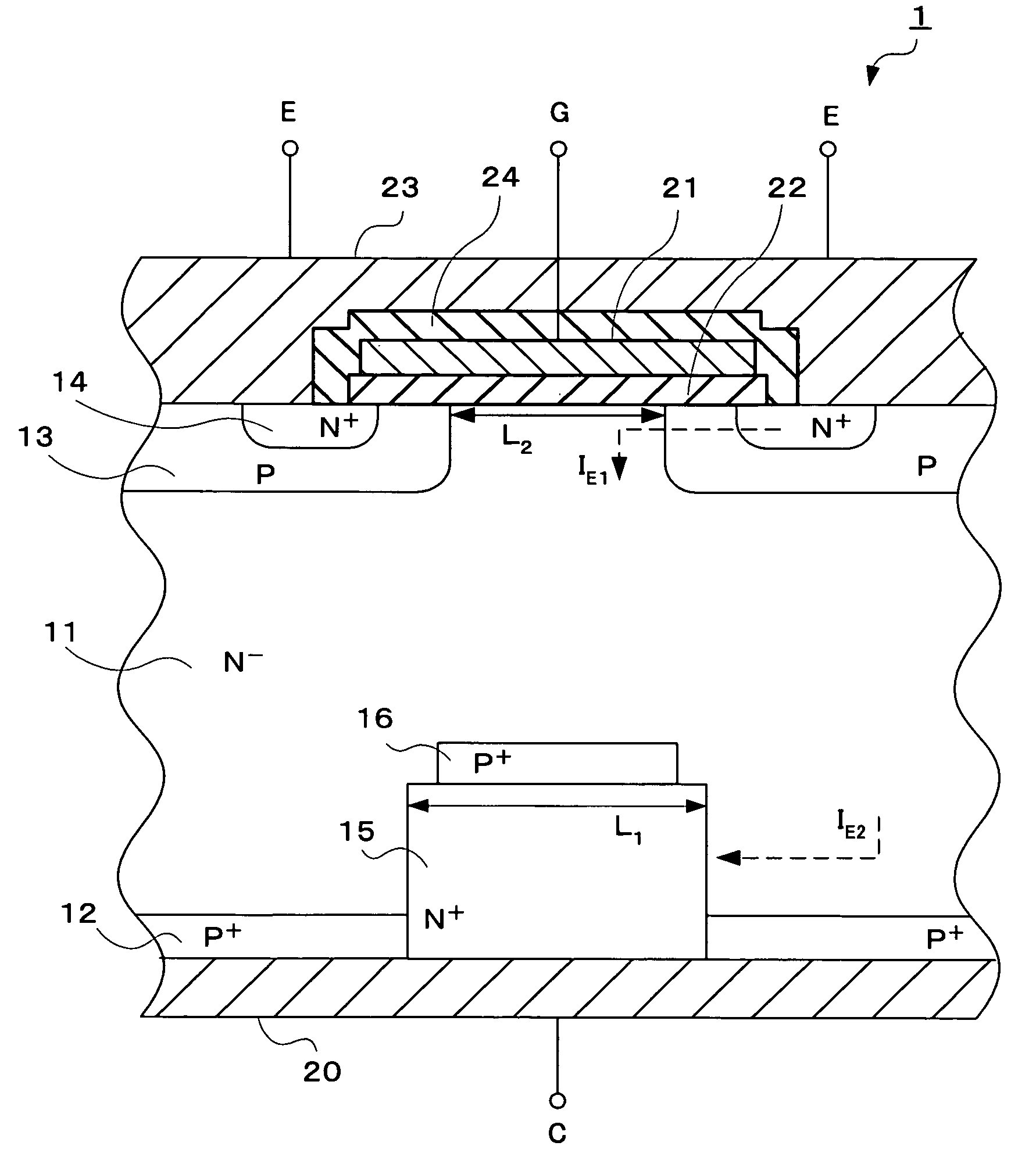
[0052]An insulated gate semiconductor device according to an embodiment of the present invention will be explained with reference to the drawings. The present embodiment will be explained by employing an example in which the insulated gate semiconductor device is an insulated gate bipolar transistor (IGBT).

[0053]The cross-sectional structure of an IGBT 1 according to the embodiment of the present invention is shown in FIG. 1.

[0054]As shown in FIG. 1, the IGBT 1 comprises an N− type base region 11 as a first semiconductor region, P+ type collector regions 12 as second semiconductor regions, P type base regions 13 as third semiconductor regions, N+ type emitter regions 14 as fourth semiconductor regions, an N+ type collector-short region 15 as a fifth semiconductor region, a P+ type semiconductor region 16 as a sixth semiconductor region, a collector electrode 20 as a first electrode, a gate electrode 21 as a control electrode, a gate insulating film 22, an emitter electrode 23 as a s...


PUM


Abstract

In an insulated gate semiconductor device (1) having an N− type base region (11), P+ type collector regions (12), P type base regions (13), and N+ type emitter regions (14), an N+ type collector-short region (15) which extends toward the N− type base region (11) farther than the P+ type collector regions (12) is formed in the lower surface of the N− type base region (11), and a P+ type semiconductor region (16) is formed between the N+ type collector-short region (15) and the N− type base region (11).

Description

TECHNICAL FIELD[0001]The present invention relates to an insulated gate semiconductor device and a method for manufacturing the same.BACKGROUND ART[0002]An insulated gate bipolar transistor (IGBT) has a high input impedance of a field effect transistor and a high current drive capability of a bipolar transistor, and is particularly suitably used as a power switching device.[0003]Conventionally, an IGBT comprises an N− type base region, a P type base region formed in a predetermined surface region of the N− type base region, an N+ type emitter region formed in a predetermined surface region of the P type base region, a P+ type collector region formed at the lower surface of the N− type base region via an N+ type buffer region, a collector electrode electrically connected to the P+ type collector region, a gate insulating film formed on a predetermined surface region of the N− type base region, a gate electrode formed on the gate insulating film, and an emitter electrode electrically ...

Claims


Application Information

Patent Timeline
Patent Type & Authority Patents(United States)
IPC IPC(8): H01L29/80H01L21/28H01L21/336H01L29/08H01L29/417H01L29/739H01L29/78
CPCH01L29/0834H01L29/7395
Inventor YOSHINOBU, KONO
Owner SANKEN ELECTRIC CO LTD
Why Eureka
Try Eureka