Piezoelectric thin-film resonator
a thin-film resonator and piezoelectric technology, applied in the direction of generators/motors, impedence networks, devices material selection, etc., can solve the problems of reducing the q value of resonance, generating spurious components, and difficult to reduce the size of the vibration uni
- Summary
- Abstract
- Description
- Claims
- Application Information
AI Technical Summary
Benefits of technology
Problems solved by technology
Method used
Image
Examples
first preferred embodiment
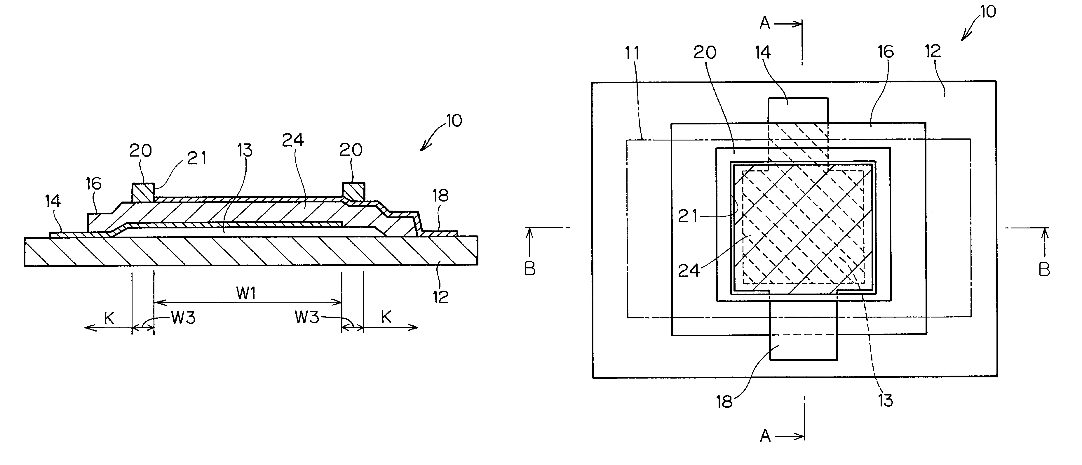
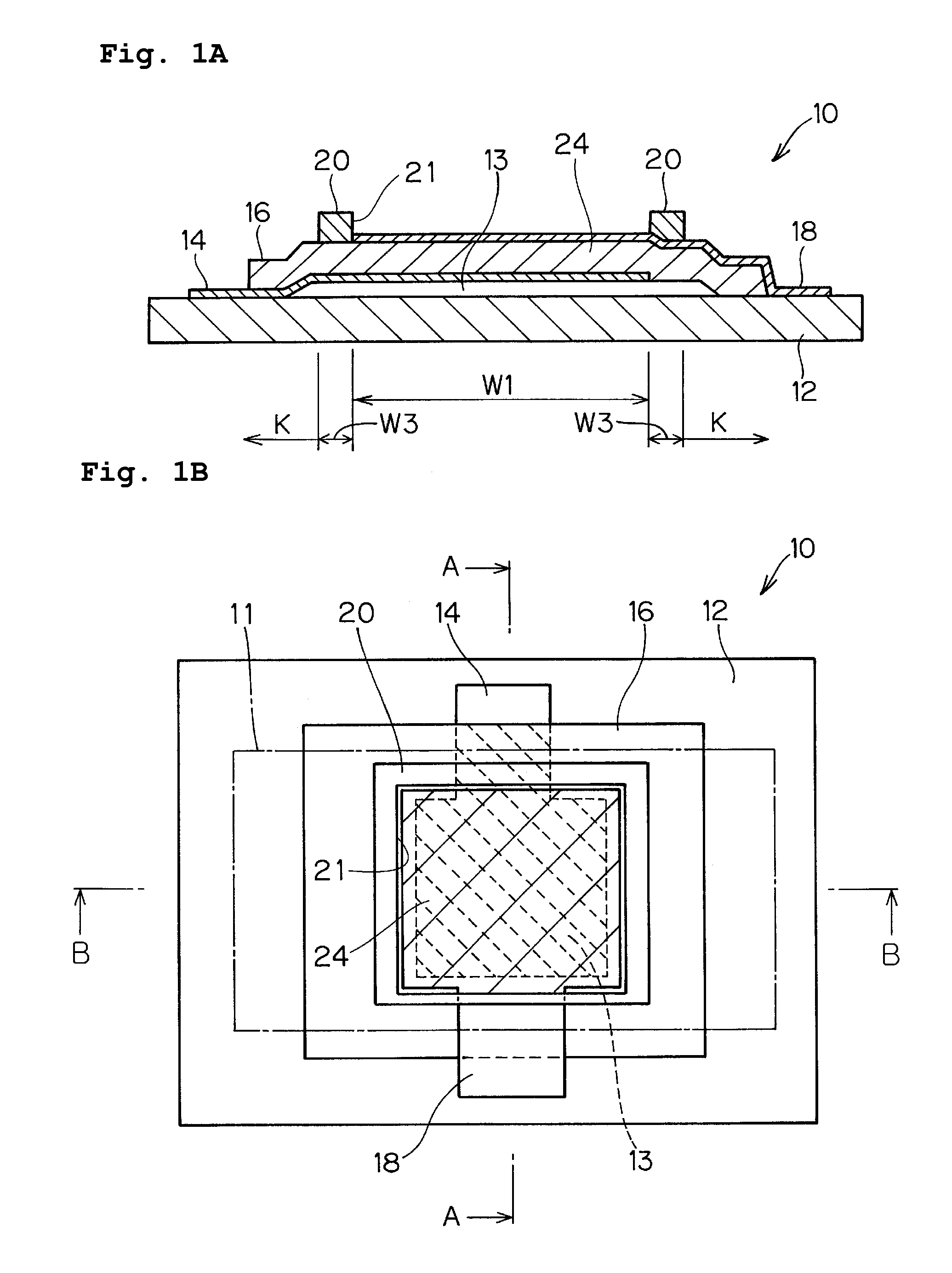
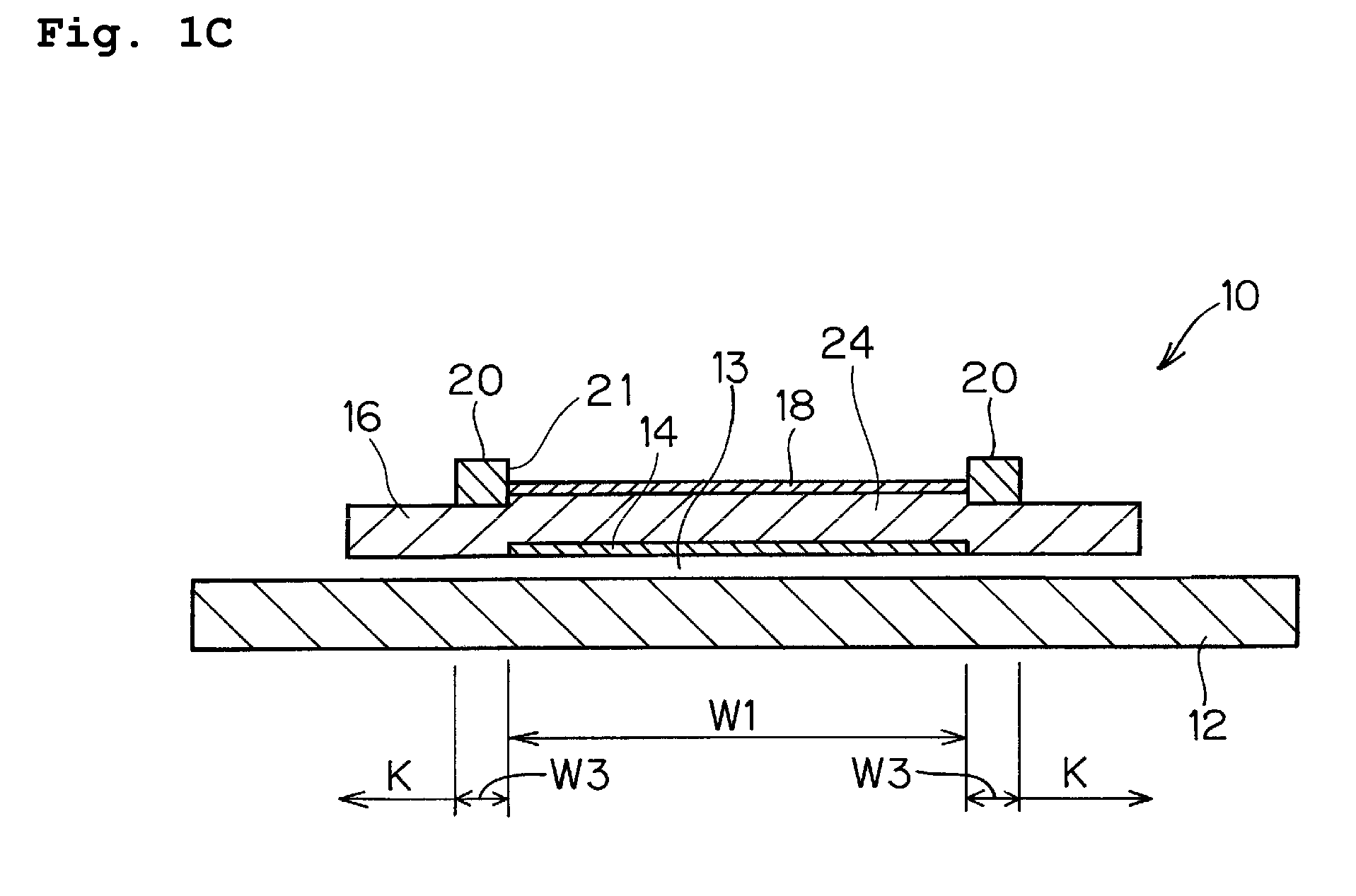
[0047]A piezoelectric resonator 10 according to a first preferred embodiment is described with reference to FIGS. 1A, 1B, 1C, and 2. FIG. 1B is a plan view. FIG. 1A is a cross-sectional view taken along a line A-A in FIG. 1B. FIG. 1C is a cross-sectional view taken along a line B-B in FIG. 1B.
[0048]As schematically shown in FIGS. 1A, 1B, and 1B, the piezoelectric resonator 10 includes a thin film unit provided on a substrate 12. That is, a lower electrode 14, a piezoelectric film 16, an upper electrode 18, and an additional film 20 are sequentially stacked on the substrate 12. The lower electrode 14 includes a portion supported by the substrate 12 and a portion raised above the substrate 12 with a gap 13 therebetween. A vibration unit 24 is provided on the raised portion. The vibration unit 24 includes the piezoelectric film 16 disposed between the lower electrode 14 and the upper electrode 18. As shown in FIG. 1B, the gap 13 is formed by disposing a sacrificial layer 11 on the subs...
second preferred embodiment
[0064]In a second preferred embodiment, the sizes and structures similar to those of the particular example of the first preferred embodiment are used except for the additional films 20. In the second preferred embodiment, the additional films 20 are made of SiO2 having a density of 2.2 g / cm3 and have thicknesses of about 200 nm, about 340 nm, about 350 nm, about 450 nm, about 520 nm, and about 530 nm.
[0065]FIG. 3 illustrates the impedance Smith charts of these piezoelectric resonators 10 including additional films 20 having these thicknesses.
[0066]A relationship between the A / B ratio and the degree of spurious suppression for the piezoelectric resonators 10 including additional films 20 having these thicknesses is shown in Table 4.
[0067]
TABLE 4B: Density ×Degree ofA: Density × ThicknessThicknessSuppression ofofofSpuriousAdditional FilmElectrodeA / B RatioComponents4408890.5X7488890.8X7708890.9◯9908891.1◯1,1448891.2◯1,1668891.3X
[0068]As shown in Table 4, when the A / B ratio is in the r...
third preferred embodiment
[0069]In a third preferred embodiment, the sizes and structures similar to those of the particular example of the first preferred embodiment are used except for the additional films 20. In the third preferred embodiment, the additional films 20 are made of Al having a density of 2.7 g / cm3 and have thicknesses of about 310 nm, about 320 nm, about 510 nm, and about 520 nm.
[0070]A relationship between the A / B ratio and the degree of spurious suppression for the piezoelectric resonators 10 including additional films 20 having these thicknesses is shown in Table 5.
[0071]
TABLE 5B: Density ×Degree ofA: Density × ThicknessThicknessSuppression ofofofSpuriousAdditional FilmElectrodeA / B RatioComponents6828890.8X8648891.0◯1,3778891.5◯1,4048891.6X
[0072]As shown in Table 5, when the A / B ratio is in the range of about 1.0 to about 1.5, the spurious components are suppressed.
PUM
 Abstract
Description
Claims
Application Information


