Electrostatic discharge device with variable on time

a technology of electric discharge device and variable time, which is applied in the direction of emergency protective arrangements for limiting excess voltage/current, transformers, electrical appliances, etc., to achieve the effect of minimizing the effects of an initial esd event, enhancing protection against subsequent esd events, and reducing the effect of initial events

Inactive Publication Date: 2009-06-09
RENESAS ELECTRONICS AMERICA
View PDF14 Cites 31 Cited by
  • Summary
  • Abstract
  • Description
  • Claims
  • Application Information

AI Technical Summary

Benefits of technology

[0014]Disclosed is an electrostatic discharge device, typically referred to as a power clamping circuit, for minimizing the effects of an initial ESD event as well as providing enhanced protection against subsequent ESD events. By using a blocking device such as a diode, the power clamping circuit is maintained in a strong “on” state for a longer duration of time that allows for faster and complete dissipation of the initial event. This strong “on” state is independent of the transient voltage of the power supply line. Further, if the device is not powered, the disclosed power clamping circuit remains in a turned “on” state, for an extended period of time, allowing for a stronger, and a more rapid response to subsequent ESD events. This enables the power clamp circuit to minimize the ESD voltage for subsequent events to a maximum voltage that is below the maximum of the ESD voltage during the initial ESD event. After an ESD event, the power clamp gate remains turned “on” for an extended period of time because the only discharge path available is gate leakage, which is very small compared to the charge stored on the gate of the clamp transistor.

Problems solved by technology

After an ESD event, the power clamp gate remains turned “on” for an extended period of time because the only discharge path available is gate leakage, which is very small compared to the charge stored on the gate of the clamp transistor.

Method used


Image

  • Electrostatic discharge device with variable on time
  • Electrostatic discharge device with variable on time
  • Electrostatic discharge device with variable on time

Examples


Embodiment Construction

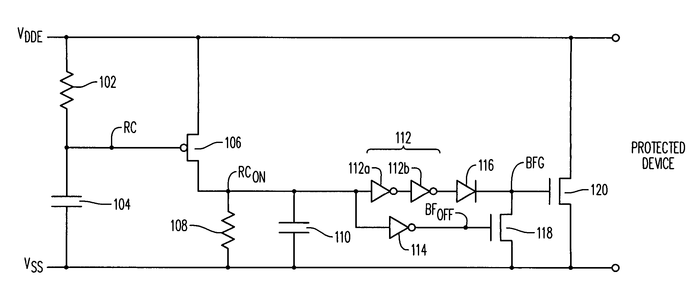
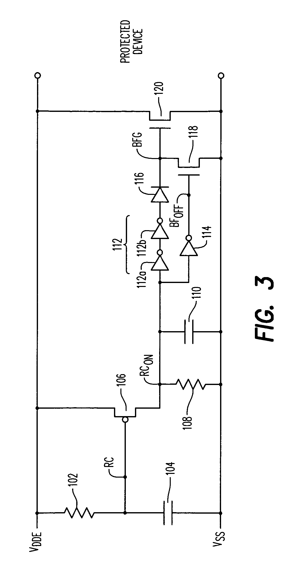
[0021]An exemplary electrostatic discharge protection device will now be described with reference to FIG. 3.

[0022]The exemplary electrostatic discharge protection device 100 for limiting the effects of an electrostatic discharge event comprises a first RC network comprising a first resistor 102 connected in series with a first capacitor 104. The first resistor is connected to the voltage rail VDDE and the first capacitor 104 is connected to the substrate voltage rail VSS. The gate terminal of a first transistor 106 is connected to a node RC between the first resistor 102 and the first capacitor 104. The source terminal of the first transistor 106 is connected to the input voltage rail VDDE. During normal conditions, e.g. prior to the onset of an ESD event, the first capacitor 104 holds the voltage at node RC to VSS, which is a low voltage, enabling the turn on of first transistor 106 when a voltage is applied to VDDE. In the illustrated embodiment, the first transistor 106 is a p-ch...


PUM


Abstract

Disclosed is an electrostatic discharge device, typically referred to as a power clamping circuit, for minimizing the effects of an initial ESD event as well as providing protection against subsequent ESD events. The power clamp is left fully turned on during and after an ESD event. Subsequent ESD events are those ESD events occurring shortly after an initial ESD event. By using a blocking device such as a diode, the power clamping circuit is maintained in a strong “on” state that fully discharges the initial ESD event and allows for a more rapid response to subsequent ESD events.

Description

FIELD OF THE INVENTION[0001]This invention relates to a power clamping circuit to limit the effects of an electrostatic discharge (ESD) event on an electronic circuit, and more particularly to a clamping circuit having a sustained on time to ensure complete dissipation of an ESD event.BACKGROUND OF THE INVENTION[0002]Electrostatic discharge (ESD) events cause numerous problems in the field of integrated circuits. The semiconductor industry has devoted a substantial amount of funds and effort into reducing the damage to integrated circuits caused by ESD events. The problems associated with an ESD event include high voltages that result in large electric fields and current densities in small semiconductor devices, such as integrated circuits. Research conducted by the semiconductor industry has shown that a fair percentage of integrated circuit failures are attributable to ESD events.[0003]A background and history of electrostatic discharge is described in ESD in Silicon Integrated Ci...

Claims


Application Information

Patent Timeline
Patent Type & Authority Patents(United States)
IPC IPC(8): H02H9/00
CPCH01L27/0285H02H9/046
Inventor TRAYNOR, KEVINDEANS, RUSSELL C.ACIERNO, VINCENT J.
Owner RENESAS ELECTRONICS AMERICA
Why Eureka
Try Eureka