
Optical near-field generating apparatus and method and information recording and reproducing apparatus

a generation apparatus and near-field technology, applied in special recording techniques, instruments, optical beam sources, etc., can solve the problems of difficult production of scatterers, etc., to increase the intensity of optical near-field, and facilitate the effect of generation

Inactive Publication Date: 2009-06-16
SONY CORP
View PDF13 Cites 12 Cited by
  • Summary
  • Abstract
  • Description
  • Claims
  • Application Information

AI Technical Summary

Benefits of technology

[0011]Thus, there may be a need for efficiently generating an optical near-field without depending on the shape of a scatterer.
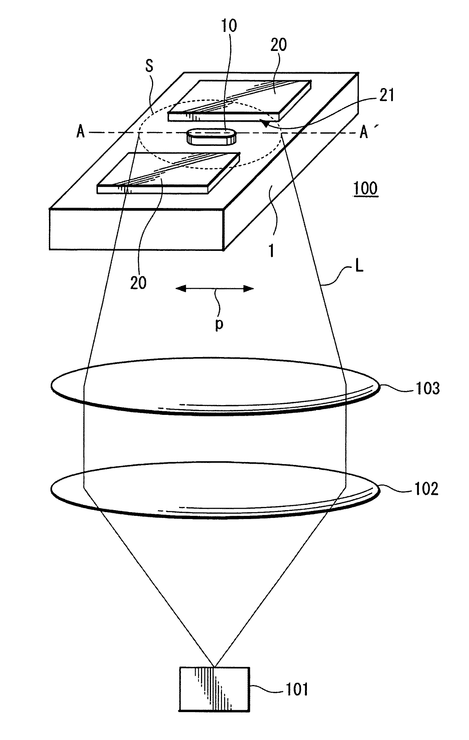
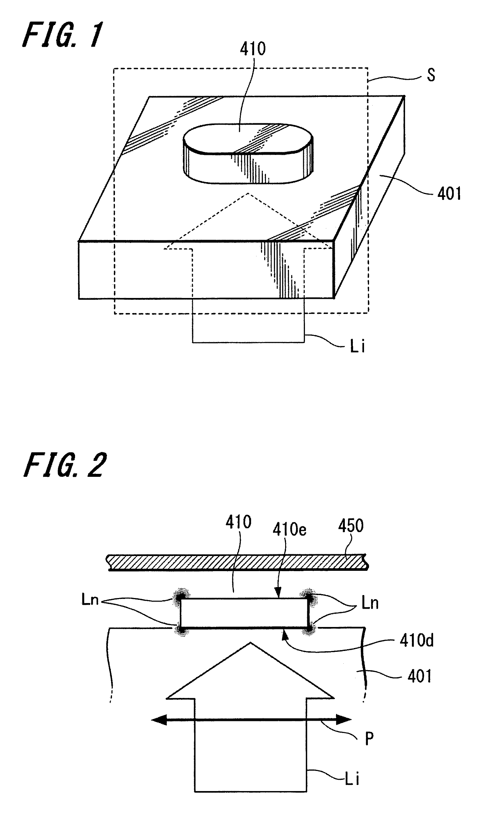
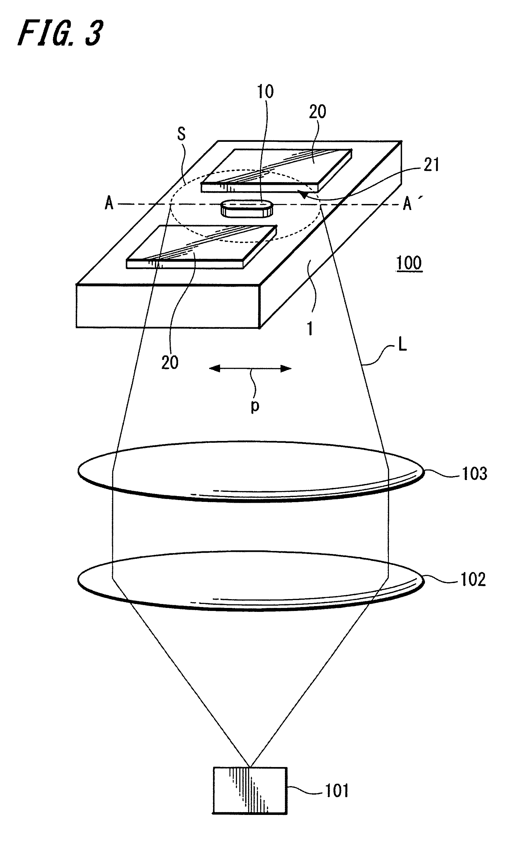
[0017]It is believed that this is because of the following reason. Generally, a surface plasmon may not be excited on a conductive body only by illumination of a light, however, when a scatterer generating a relatively strong optical near-field is arranged in the vicinity of the conductive body, the charge phase distribution on the surface of the conductive body is also influenced in the form of coupling by the strong optical near-field on the surface of the scatterer to be determined. Therefore, under a certain condition, the surface plasmon is excited on the surface of the conductive body. As a result, the energy of the incident light is converted into the surface plasmons on the surfaces of the scatterer and the conductive body, and because those surface plasmons are electro-magnetically coupled with each other, the intensity of the optical near-field being generated on the surface of the scatterer is increased.
[0018]Accordingly, according to an embodiment of the invention, without complicating the shape configuration of the scatterer itself, that is, without complicating the manufacture of the scatterer, by arranging a conductive body in the vicinity of the scatterer under an appropriate condition, it becomes possible to surely increase the intensity of an optical near-field to be generated on the surface of the scatterer, as compared with a case that the conductive body is not provided.
[0019]According to the optical near-field generating apparatus, the optical near-field generating method and the information recording / reproducing apparatus according to embodiments of the invention, it becomes possible to easily generate a relatively highly efficient optical near-field without depending on the shape of the scatterer.

Problems solved by technology

Accordingly, there is a problem that manufacture of the scatterers becomes very difficult and putting the scatterers into high-volume production is very difficult.

Method used


Image

  • Optical near-field generating apparatus and method and information recording and reproducing apparatus
  • Optical near-field generating apparatus and method and information recording and reproducing apparatus
  • Optical near-field generating apparatus and method and information recording and reproducing apparatus

Examples


first embodiment

[0085]First, regarding the cases that the conductive body 20 is arranged as illustrated in FIG. 10A and FIG. 10B and FIG. 12, examples in which the shape of the scatterer 10 is changed are described. In each example, how the multiplication factor of the peak intensity of an optical near-field changes has been examined. In this example, as illustrated in a schematic cross section of FIG. 16, the scatterer 10 in an approximately rectangular shape in cross section and 30 nm thick is arranged on the substrate 1 made of SiO2, and a 6 nm thick thin TbFeCo film 32 is arranged over the scatterer 10 (and the substrate 1) through an 8 nm gap 31. The planar shape of the scatterer 10 is changed as illustrated in FIG. 17A through FIG. 17D, and the peak intensity of each optical near-field has been calculated. In the example of FIG. 17A, the scatterer 10 is in a planar rectangular shape, and the length l in the direction parallel to the polarizing direction of incident light is 70 nm, and the wid...

second embodiment

[0090]Next, with respect to examples in which the materials of the scatterer 10 and the substrate 1 and the wavelength of the incident light have been changed, how the multiplication factor of the peak intensity of each optical near-field changes has been similarly examined. FIG. 20A through FIG. 20D are planar views illustrating examples of the scatterer 10. In the examples illustrated in FIG. 20A through FIG. 20D, the scatterer 10 is in a rod-like shape. In the example illustrated in FIG. 20A, the length l of the scatterer 10 is 100 nm, the width w is 24 nm, the material of the scatterer 10 is silver, the material of the substrate 1 is quartz, and the wavelength of the incident light is 780 nm. In the example illustrated in FIG. 20B, the length l of the scatterer 10 is 100 nm, the width w is 24 nm, the material of the scatterer 10 is gold, the material of the substrate 1 is quartz, and the wavelength of the incident light is 780 nm. In the example illustrated in FIG. 20C, the leng...

third embodiment

[0098]Next, regarding a case that plural scatterers are provided, description is made with respect a result of examining the amplification effect of an optical near-field based on arrangement of conductive bodies.

[0099]A method has been known in which a second scatterer is arranged in the vicinity of a tip end of a scatterer in which an optical near-field is generated to amplify the intensity of the optical near-field. In the example below, as illustrated in FIG. 23, two scatterers, scatterers 10A and 10B, are arranged on the substrate 1. Each of the scatterers 10A and 10B is formed in a rod-like planar shape, and the width is 24 nm, the length l along the polarizing direction of the incident light is 90 nm, and the thickness is 30 nm. A peak-to-peak distance ds between the scatteres 10A and 10B is 20 nm. The conductive bodies 20 in the shapes similar to those of the example of FIG. 10A and FIG. 10B are arranged for the scatterers 10A and 10B, and the multiplication factor of the in...


PUM

PropertyMeasurementUnit
angleaaaaaaaaaa
angleaaaaaaaaaa
angleaaaaaaaaaa

Abstract

An optical near-field generating apparatus includes a conductive scatterer causing an optical near-field based on a surface plasmon to be generated by being illuminated by incident light, and a conductive body arranged in a vicinity of the scatterer and generating a surface plasmon by being illuminated by the incident light and by being influenced by the surface plasmon of the scatterer. An oscillation direction of the surface plasmon of the conductive body is approximately parallel to an oscillation direction of the surface plasmon of the scatterer, and a generation region of the surface plasmon of the conductive body exists in a position deviated from a region extending in an oscillation direction of the surface plasmon of the scatterer.

Description

CROSS REFERENCES TO RELATED APPLICATIONS[0001]The invention contains subject matter related to Japanese Patent Application JP 2007-029796 filed in the Japanese Patent Office on Feb. 8, 2007, the entire contents of which being incorporated herein by reference.BACKGROUND OF THE INVENTION[0002]1. Field of the Invention[0003]The invention relates to an optical near-field generating apparatus generating an optical near-field by illuminating a light to a scatterer composed of a conductive material, a method of generating an optical near-field, and an information recording and reproducing apparatus.[0004]2. Description of the Related Art[0005]Recently, as a method of forming a minute optical spot exceeding a diffraction limit of a light, use of a local electromagnetic field called an optical near-field is drawing attention. For example, in the field of an information recording apparatus, heat assisting electromagnetic recording using a minute optical spot formed by using the optical near-f...

Claims


Application Information

Patent Timeline
Patent Type & Authority Patents(United States)
IPC IPC(8): G11B5/02G11B11/24G11B9/12G11B13/08G11B7/125
CPCB82Y10/00B82Y20/00G11B5/02G11B7/1387G11B5/314G11B2005/0021G11B2005/0005G11B7/127
Inventor HONGO, KAZUHIROWATANABE, TETSU
Owner SONY CORP
Learn More