Impedance control circuit in semiconductor device and impedance control method

a technology of impedance control and semiconductor devices, applied in logic circuit coupling/interface arrangements, pulse techniques, instruments, etc., can solve the problems of impedance mismatch, degraded signal, noise increase, etc., and achieve the effect of improving the transmission error of output signal or the setup/hold failure in the receiver without increasing the resolution

Active Publication Date: 2009-06-16
SAMSUNG ELECTRONICS CO LTD
View PDF8 Cites 2 Cited by
  • Summary
  • Abstract
  • Description
  • Claims
  • Application Information

AI Technical Summary

Benefits of technology

[0019]An exemplary embodiment of the present invention provides an impedance control circuit of semiconductor device and an impedance control method, through which an impedance mismatch between pull-up and pull-down resistances can be reduced without increasing a resolution. Furthermore, a mismatch between pull-up and pull-down resistances reduced by half a digital control resolution within pull-up and pull-down transistor arrays, thus transmission error of an output signal or a setup / hold fail in a receiver can be improved.

Problems solved by technology

However, when the swing width of the signal is reduced, an influence of external noise increases, and a reflection of the output signal caused by impedance mismatch degrades the signal.
Impedance mismatch can be caused by a number of factors, including external noise, or variations in power source voltage, operating temperatures and fabricating processes, etc.
When output impedance(ZQ) or chip termination(ZT) controls are not performed properly, impedance mismatch occurs and both transmitted and received signals may be distorted, causing a number of potential problems.
As an example, when a semiconductor device receives a distorted output signal through a receiver, a setup / hold fail or a decision error from improper input level may occur
In a semiconductor memory device employing such a scheme, it is frequently difficult to obtain and adaptively correct a precise output impedance value, due to many conditions such as varying power source voltages, operating temperatures, and manufacturing processes.
When a mismatch of pull-up and pull-down resistances occurs within the transistor array of the terminator, the median signal is changed, having an adverse effect on a setup / hold window of the receiver.
In a prior art, there is an impedance mismatch of a 1-bit resolution between pull up and down resistances which limits the reduction in impedance mismatch that can occur.
Consequently, when a mismatch between pull-up and pull-down resistances occurs, transmission error of output signals occurs or a median input signal is changed, potentially causing a setup / hold fail in a receiver.

Method used


Image

  • Impedance control circuit in semiconductor device and impedance control method
  • Impedance control circuit in semiconductor device and impedance control method
  • Impedance control circuit in semiconductor device and impedance control method

Examples


Embodiment Construction

[0032]Hereinafter, exemplary embodiments of the present invention will be described in detail with reference to the attached drawings. Like reference numerals in the drawings denote like elements.

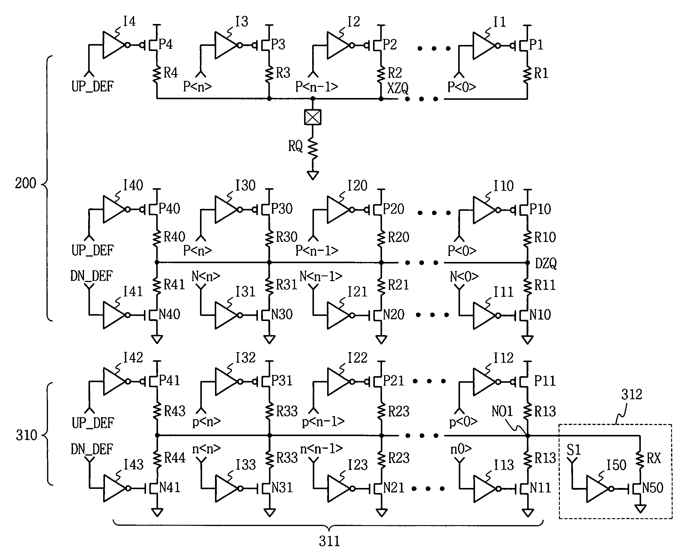
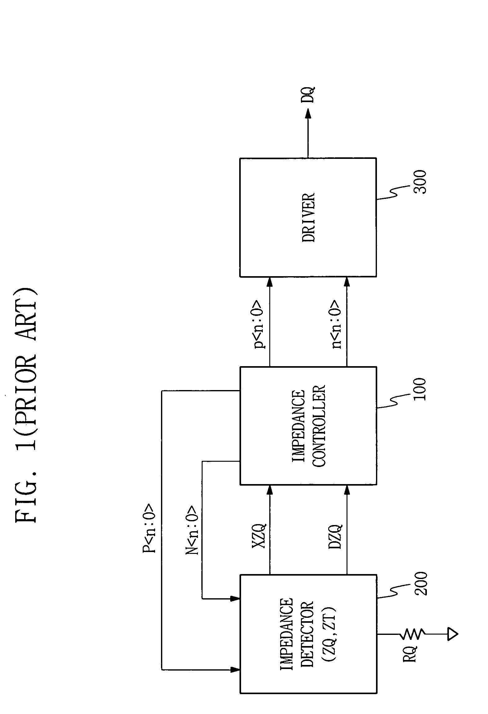
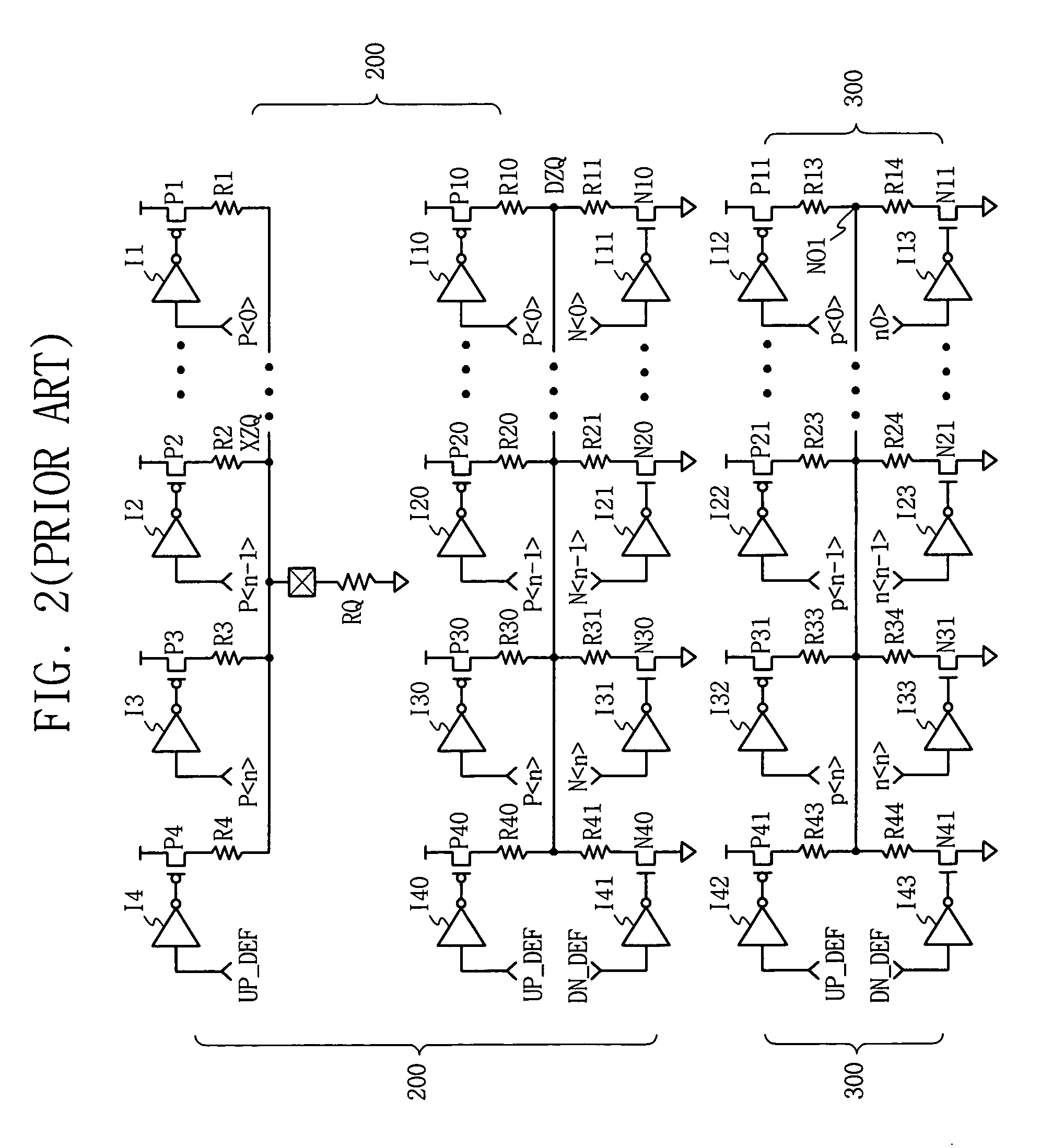
[0033]FIG. 4 is a circuit diagram illustrating an exemplary embodiment of the invention. An impedance detector 200 outputs a pull-up output value XZQ to a detection pad connected between an external determination resistor RQ and a pull-up transistor array P1-P4 in response to a pull-up control code data P, and outputs a pull-down output value DZQ to a resistance divider terminal commonly connected between pull-up and pull-down transistor arrays P10, P20-P40 and N10, N20-N40 in response to the pull-up control code data P and the pull-down control code data N.

[0034]A driver 310 functioning as an output driver or terminator includes transistor arrays P11, P21-P41 and N11, N21-N41 the same as the pull-up and pull-down transistor arrays of the impedance detector 200. Transistors within the trans...


PUM


Abstract

An impedance control circuit includes an impedance detector, an output driver and an impedance controller. The impedance detector generates a first output value to a detection pad connected between an external determination resistor and a pull-up transistor array, and outputs a second output value to a resistance divider terminal commonly connected between a pull-up and pull-down transistor array in response to a pull-up control code data and a pull-down control code data. The output driver has a commonly connected pull-up and pull-down transistor array, and a compensating unit connected to the pull-up and pull-down transistor array of the output driver, to compensate for quantization error of the pull-up and pull-down control code data. The impedance controller performs a comparison and counting operation so that the first and second output values of the impedance detector become approximated to a predetermined reference value, and generates the pull-up and pull-down control code data.

Description

CROSS-REFERENCE TO RELATED PATENT APPLICATION[0001]This application claims priority to Korean Patent Application No. 2005-0039153, filed on May 11, 2005, in the Korean Intellectual Property Office, the disclosure of which is incorporated by reference herein.BACKGROUND OF THE INVENTION[0002]1. Field of the Invention[0003]The present invention relates to a field of impedance control for semiconductor devices, and more particularly, to an impedance control circuit and method in a semiconductor device, capable of reducing an impedance mismatch.[0004]2. Discussion of the Related Art[0005]A semiconductor device typically includes pins to transmit and send data to and from other devices, and a data output circuit which functions as a data output buffer and a driver circuit to provide internal data to external devices. As an example, the pins may be connected to a transmission line such as printed wiring provided on a mounting substrate, in a semiconductor device incorporated into an electr...

Claims


Application Information

Patent Timeline
Patent Type & Authority Patents(United States)
IPC IPC(8): H03K17/16H03K19/003H03K5/12
CPCH03K19/0005G11C7/1051G11C7/22G11C11/413
Inventor KIM, TAE-HYOUNGKWON, JI-SUKCHO, UK-RAE
Owner SAMSUNG ELECTRONICS CO LTD
Why Eureka
Try Eureka