Supercharge Your Innovation With Domain-Expert AI Agents!

Plasma etching of Cu-containing layers

a technology of cu-containing layers and plasma, which is applied in the direction of electrical discharge tubes, decorative arts, electrical equipment, etc., can solve the problems of difficulty in defining extremely fine features, limiting the ability to batch-fabricate sub-micron magnetic devices, and challenging cu-cmp technology

Inactive Publication Date: 2009-06-30
TOKYO ELECTRON LTD
View PDF6 Cites 6 Cited by
  • Summary
  • Abstract
  • Description
  • Claims
  • Application Information

AI Technical Summary

Problems solved by technology

However, Cu CMP technology is challenging and it has difficulty defining extremely fine features.
The lack of suitable fast etching processes for materials such as Cu and various magnetic materials, can limit the ability to batch-fabricate sub-micron magnetic devices.
Patterning of magnetic devices has been predominantly accomplished using Ar+-ion milling or additive deposition processes such as electroplating or lift-off, but these methods are undesirable for semiconductor batch processing.
The etching rates with this method are very low and another drawback is that the sputtered CUClx coats the chamber walls and this requires periodic cleaning of the chamber.
An equally serious problem is encountered when high-aspect-ratio features are etched in chlorine plasma and the sputtered CuClx products redeposit on the feature sidewalls where the effects of physical sputtering are reduced.
Furthermore, when the process is carried out at elevated temperatures (>200° C.) to increase the volatility of the reacted Cu layer, corrosion can occur due to accumulated CuClx etch residues on the surface.
If these residues are not removed by a post-etch cleaning step, they can cause continuing corrosion of the Cu even after the application of a protective layer over the etched features.
These alternative approaches are not practical for semiconductor batch processing of large substrates due to poor etch uniformity, high cost and added equipment complexity, and reliability problems.
Both of the abovementioned patents involve forming etching reactants in-situ during the process, which can result in poor control over the delivery of the etching reactant to the surface of the metal film to be etched.

Method used


Image

  • Plasma etching of Cu-containing layers
  • Plasma etching of Cu-containing layers
  • Plasma etching of Cu-containing layers

Examples


Embodiment Construction

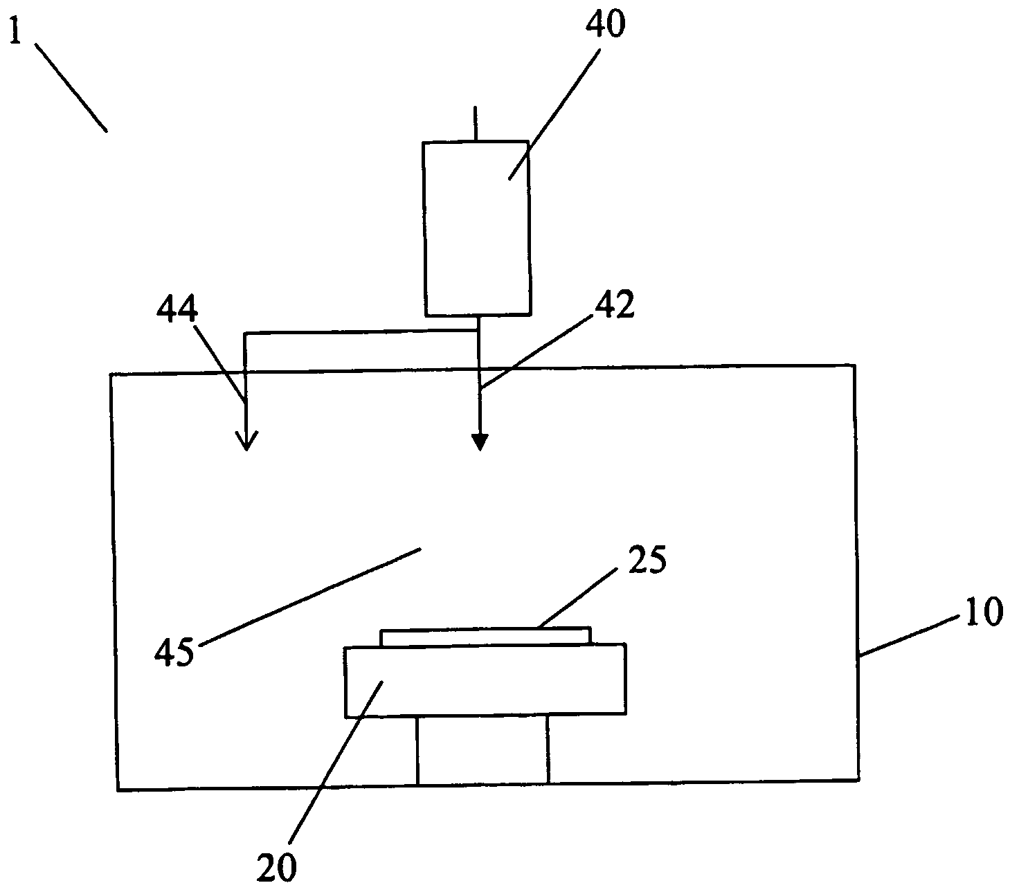
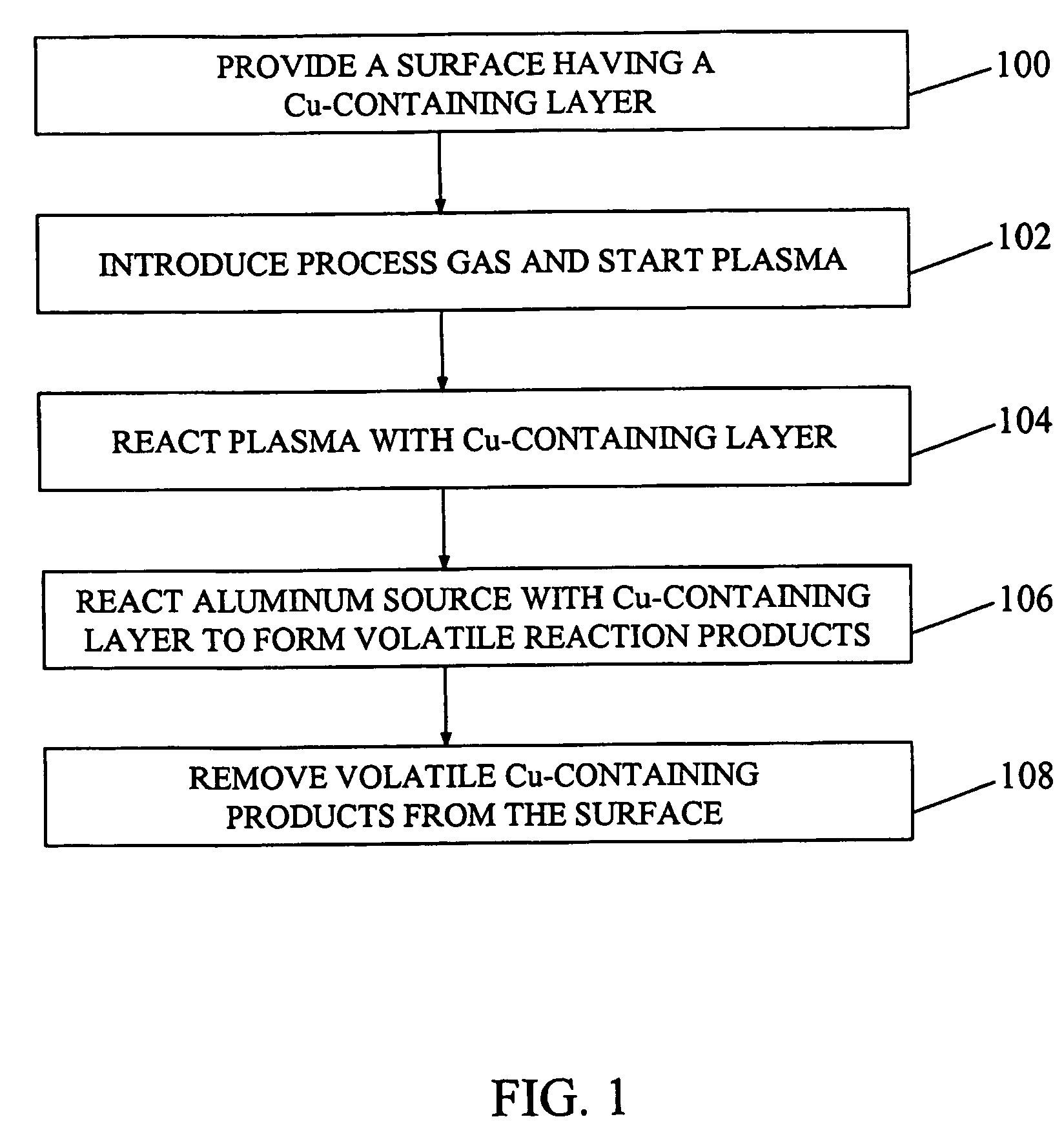
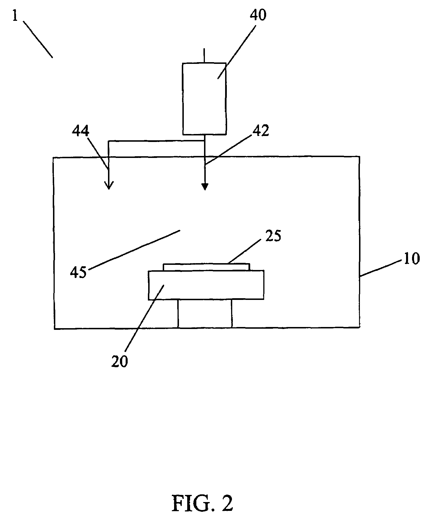
[0024]In general, the present invention pertains to a plasma processing method for etching pure Cu layers, Al—Cu alloys, and other Cu-based alloys for manufacturing an integrated circuit.

[0025]The method uses a plasma process that comprises a reactive halogen species and an aluminum source to etch Cu-containing layers by forming volatile reaction products that are removed by ion-assisted etching.

[0026]For example, the reactive halogen species can be formed from a chlorine-containing gas that is selected from the group containing Cl2, HCl, BCl3, SiCl4, CHCl3, CCl4, and mixtures thereof. Reactive halogen species can also be formed from non-chlorine containing gases such as aluminum bromide.

[0027]Al layers used in integrated circuits commonly contain a small amount of Cu (2—Al2Cl6. A reduced etch rate for Al—Cu layer with high Cu content is possibly due to a limited supply of aluminum chloride from the etching of Al in the Al—Cu film, that is available for reacting (complexing) with th...


PUM

PropertyMeasurementUnit
temperatureaaaaaaaaaa

Abstract

A method and apparatus are provided for plasma etching of Cu-containing layers in semiconductor devices using an aluminum source in the presence of a halogen-containing plasma. The aluminum source reacts with halogenated Cu-containing surfaces and forms volatile etch products that allows for anisotropic etching of Cu-containing layers using conventional plasma etching tools.

Description

CROSS-REFERENCE TO RELATED APPLICATIONS[0001]The present application claims priority and is related to U.S. application Ser. No. 60 / 379,754, filed on May 14, 2002. The present application is also related to U.S. application Ser. No. 60 / 392,045, filed on Jun. 28, 2002. The entire contents of both of those applications are herein incorporated by reference.FIELD OF THE INVENTION[0002]The present invention relates to plasma etching of copper-containing layers used in semiconductor applications.BACKGROUND OF THE INVENTION[0003]Copper (Cu) is emerging as the metal of choice in a wide variety of semiconductor applications. Lower electrical resistivity, coupled with improved electromigration performance and increased stress migration resistance are important material properties that favor the use of Cu over aluminum (Al) in interconnect lines and contacts. The lower electrical resistance is critical since it allows signals to move faster by reducing the RC time delay. The superior resistanc...

Claims


Application Information

Patent Timeline
Patent Type & Authority Patents(United States)
IPC IPC(8): C23F1/00H01L21/3213
CPCH01J37/32082H01L21/32136
Inventor LUDVIKSSON, AUDUNNCHEN, LEE
Owner TOKYO ELECTRON LTD
Features
  • R&D
  • Intellectual Property
  • Life Sciences
  • Materials
  • Tech Scout
  • Unparalleled Data Quality
  • Higher Quality Content
  • 60% Fewer Hallucinations
Learn More