Process for forming thin film encapsulation layers

a technology of encapsulation layer and thin film, which is applied in the direction of coating, solid-state device, chemical vapor deposition coating, etc., can solve the problems of oled materials being subject to degradation, affecting the performance of oled materials, and affecting the quality of oled materials,

Inactive Publication Date: 2009-03-26
EASTMAN KODAK CO
View PDF14 Cites 44 Cited by
  • Summary
  • Abstract
  • Description
  • Claims
  • Application Information

AI Technical Summary

Benefits of technology

[0040]It is an advantage of the present invention that it provides an advantageous process for atomic layer deposition of a metal-oxide-based layers onto a substrate, well suited to a number of different types of substrates and deposition environments.
[0041]It is yet a further advantage of the present invention that it is adaptable for deposition on a web or other moving substrate, including deposition onto a large area substrate.
[0042]It is a further advantage of the present invention that it allows operation, in preferred embodiments, under atmospheric pressure conditions.
[0043]It is still a further advantage of the present invention that it can be employed in low temperature processes at atmospheric pressures, which processes may be practice in an unsealed environment, open to ambient atmosphere.

Problems solved by technology

However, the materials comprising the organic EL element are sensitive and, in particular, are easily destroyed by moisture and high temperatures (for example greater than 140 degrees C.).
The described sputter deposited electrode layers, as well as underlying layers, typically are not sufficiently impermeable to environmental contaminants when employed as the transparent top electrode in a top-emitting device, necessitating the use of additional encapsulating overcoat layers or sealed transparent glass covers, thereby exacerbating problems with light trapping and / or increased costs for such devices.
It is well known that OLED materials are subject to degradation in the presence of environmental contaminants, in particular moisture.
In contrast, typically polymeric materials have a moisture permeation rate of approximately 0.1 gm / m2 / day and cannot adequately protect the OLED materials without additional moisture blocking layers.
However, such protective layers also cause additional problems with light trapping in the layers since they may be of lower index than the light-emitting organic layers.
These items increase the capital cost of systems and preclude the easy use of continuous web based systems.
In practice in any process it is difficult to avoid some direct reaction of the different precursors leading to a small amount of chemical vapor deposition reaction.
Self-saturating surface reactions make ALD insensitive to transport non-uniformities, which might otherwise impair surface uniformity, due either to engineering tolerances and the limitations of the flow process or related to surface topography (that is, deposition into three dimensional, high aspect ratio structures).
As a general rule, a non-uniform flux of chemicals in a reactive process generally results in different completion times at different areas.
Existing ALD approaches have been compromised with the trade-off between the need to shorten reaction times and improve chemical utilization efficiency, and on the other hand, the need to minimize purge-gas residence and chemical removal times. One approach to overcome the inherent limitations of time depended ALD systems is to provide each reactant gas continuously and to move the substrate through each gas in succession.
While processes such as those described in the '563 Yudovsky and '022 Suntola et al. patents may avoid some of the difficulties inherent to pulsed gas approaches, these processes have other drawbacks.
For example, it would be very difficult to maintain a uniform vacuum at different points in an array and to maintain synchronous gas flow and vacuum at complementary pressures, thus compromising the uniformity of gas flux that is provided to the substrate surface.
Despite the usefulness and ease of use of these spatially dependent ALD systems, they continue to be less capable than time dependent ALD systems in terms of separation of the mutually reactive gases.

Method used


Image

  • Process for forming thin film encapsulation layers
  • Process for forming thin film encapsulation layers
  • Process for forming thin film encapsulation layers

Examples


examples

Description of the Coating Apparatus

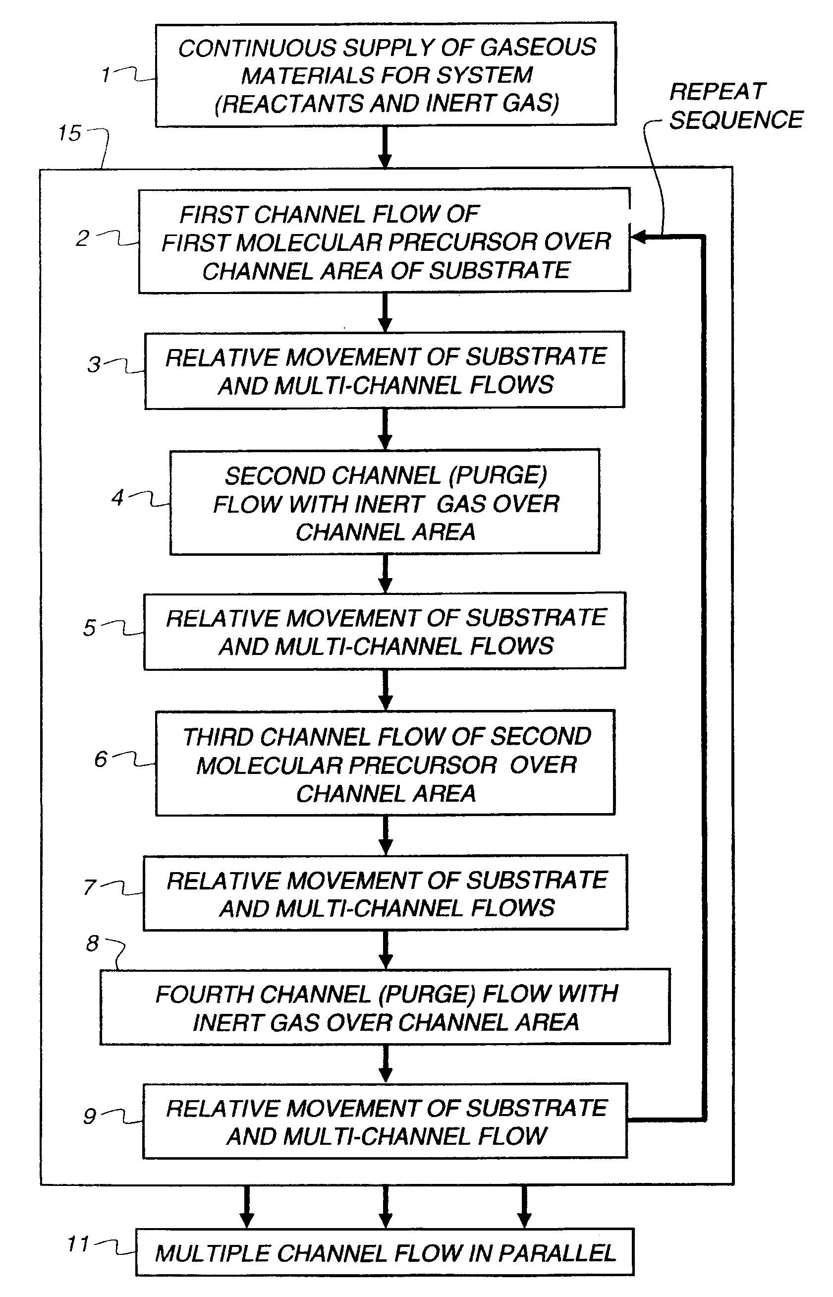
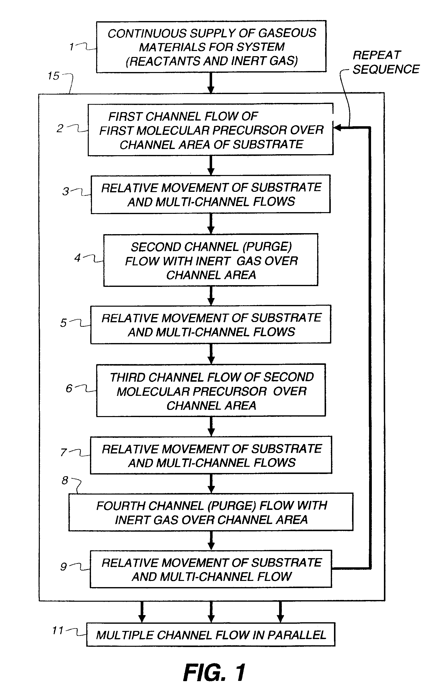
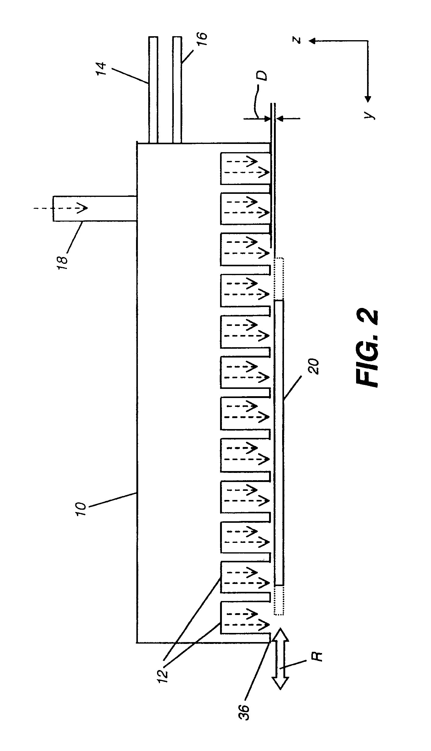
[0147]All of the following thin film examples employ a coating apparatus, for atomic layer deposition, having the flow setup indicated in FIG. 3, which is a block diagram of the source materials for a thin film deposition process according to the Examples.

[0148]The flow setup is supplied with nitrogen gas flow 81 that has been purified to remove oxygen and water contamination to below 1 ppm. The gas is diverted by a manifold to several flow meters which control flows of purge gases and of gases diverted through bubblers to select the reactive precursors. In addition to the nitrogen supply, air flow 90 is also delivered to the apparatus. The air is pretreated to remove moisture.

[0149]The following flows are delivered to the ALD coating apparatus: metal (zinc) precursor flow 92 containing metal precursors diluted in nitrogen gas; oxidizer-containing flow 93 containing non-metal precursors or oxidizers diluted in nitrogen gas; and nitrogen purge flow...

##ventive example 1

Inventive Example 1

[0182]Various multilayers of a Al2O3 / ZnO stack, wherein the number and thickness of the layers were varied were made and tested. The multilayer stacks were about 2000 Å in total thickness. The coating for these two inventive devices comprised the following combination of layers:

Al2O3120 ÅZnO100 ÅAl2O3100 ÅZnO150 ÅAl2O3200 ÅZnO200 ÅAl2O31000 Å 

[0183]The results showed that the multilayered film stacks consisting of Al2O3 and ZnO layers exhibited less or no cracks, meaning that the stress was better accommodated by the multilayer film stacks.

[0184]It was also shown that the multilayered Al2O3 / ZnO film stacks can provide good protection: two of the inventive devices exhibited no dark spot growth in the center of the OLED pixels (edge growth can be eliminated by optimization of the geometry and the flow rates) after 24 and 48 hours in a humidity chamber.

##ventive example 2

Inventive Example 2

[0185]An OLED device was coated with an encapsulation film containing a mixture of Al2O3 / ZnO prepared by combining precursors for two oxides in the microchamber slots of a spatially dependent atomic layer deposition head, using water in another channel.

[0186]A total of 450 oscillation cycles of the delivery head was performed. During the coating process, a 120 Å layer of pure Al2O3 was first deposited. Then the flows of metal precursors to the trimethylaluminum bubbler flow and to the diethylzinc bubbler flow were gradually modified to increase the relative amount of ZnO and decrease the relative amount of Al2O3 until the film reached 100% of ZnO. Then the process was repeated in the opposite direction, diminishing the relative amount of ZnO while increasing the relative amount of Al2O3 such that the final 100 Å of material consisted of Al2O3 only. The total thickness of the mixed Al2O3 / ZnO film was approximately 2000 Å.

[0187]After the coating process was complete...


PUM

PropertyMeasurementUnit
temperatureaaaaaaaaaa
speedaaaaaaaaaa
humidityaaaaaaaaaa

Abstract

A process is disclosed for making a thin film encapsulation package for an OLED device by depositing a thin film material on an OLED device to be encapsulated, comprising simultaneously directing a series of gas flows along substantially parallel elongated output openings, wherein the series of gas flows comprises, in order, at least a first reactive gaseous material, an inert purge gas, and a second reactive gaseous material, optionally repeated a plurality of times, wherein the first reactive gaseous material is capable of reacting with a substrate surface treated with the second reactive gaseous material to form an encapsulating thin film, wherein the first reactive gaseous material is a volatile organo-metal precursor compound. The process is carried out substantially at or above atmospheric pressure, and the temperature of the substrate during deposition is under 250° C.

Description

CROSS-REFERENCE TO RELATED APPLICATIONS[0001]Reference is made to commonly assigned U.S. patent application Ser. No. 11 / 616,536 filed Dec. 27, 2006, entitled “OLED WITH PROTECTIVE ELECTRODE” by Ronald Steven Cok, U.S. application Ser. No. 11 / 392,007, filed Mar. 29, 2006 by Levy and entitled, “PROCESS FOR ATOMIC LAYER DEPOSITION,” U.S. application Ser. No. 11 / 392,006, filed Mar. 29, 2006 by Levy and entitled “APPARATUS FOR ATOMIC LAYER DEPOSITION,” U.S. application Ser. No. 11 / 620,738, filed Jan. 8, 2007 by Levy and entitled “DELIVERY DEVICE FOR DEPOSITION,” U.S. application Ser. No. 11 / 620,740, filed Jan. 8, 2007 by Nelson et al. and entitled “DELIVERY DEVICE COMPRISING GAS DIFFUSER FOR THIN FILM DEPOSITION,” U.S. application Ser. No. 11 / 620,744, filed Jan. 8, 2007 by Levy and entitled, “DEPOSITION SYSTEM AND METHOD USING A DELIVERY HEAD SEPARATED FROM A SUBSTRATE BY GAS PRESSURE,” U.S. application Ser. No. 11 / 627,525 (docket 93187), filed Jan. 26, 2007 by Peter Cowdery-Corvan et al...

Claims


Application Information

Patent Timeline
Patent Type & Authority Applications(United States)
IPC IPC(8): B05D5/12
CPCC23C16/403C23C16/405H01L51/5237C23C16/45574C23C16/45551H10K50/844B05D5/00
Inventor FEDOROVSKAYA, ELENA A.BOROSON, MICHAEL L.LEVY, DAVID H.AGOSTINELLI, JOHN A.
Owner EASTMAN KODAK CO
Why Eureka
Try Eureka