
Semiconductor device having a pair of fins and method of manufacturing the same

a technology of semiconductor and fin, which is applied in the direction of semiconductor devices, semiconductor/solid-state device details, electrical apparatus, etc., can solve the problems of relatively expensive soi substrates, etc., and achieve the effect of reducing short channel effect, and reducing disturbances during reading operations

Inactive Publication Date: 2009-07-14
SAMSUNG ELECTRONICS CO LTD
View PDF27 Cites 17 Cited by
  • Summary
  • Abstract
  • Description
  • Claims
  • Application Information

AI Technical Summary

Benefits of technology

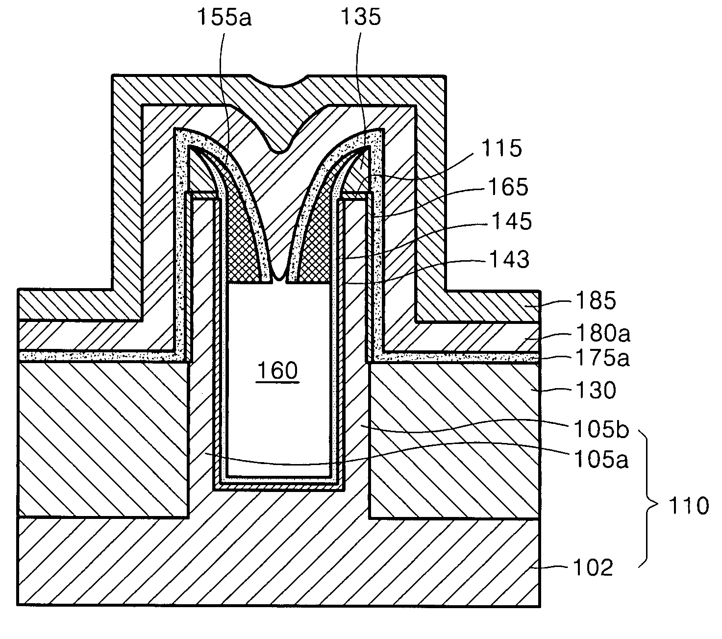
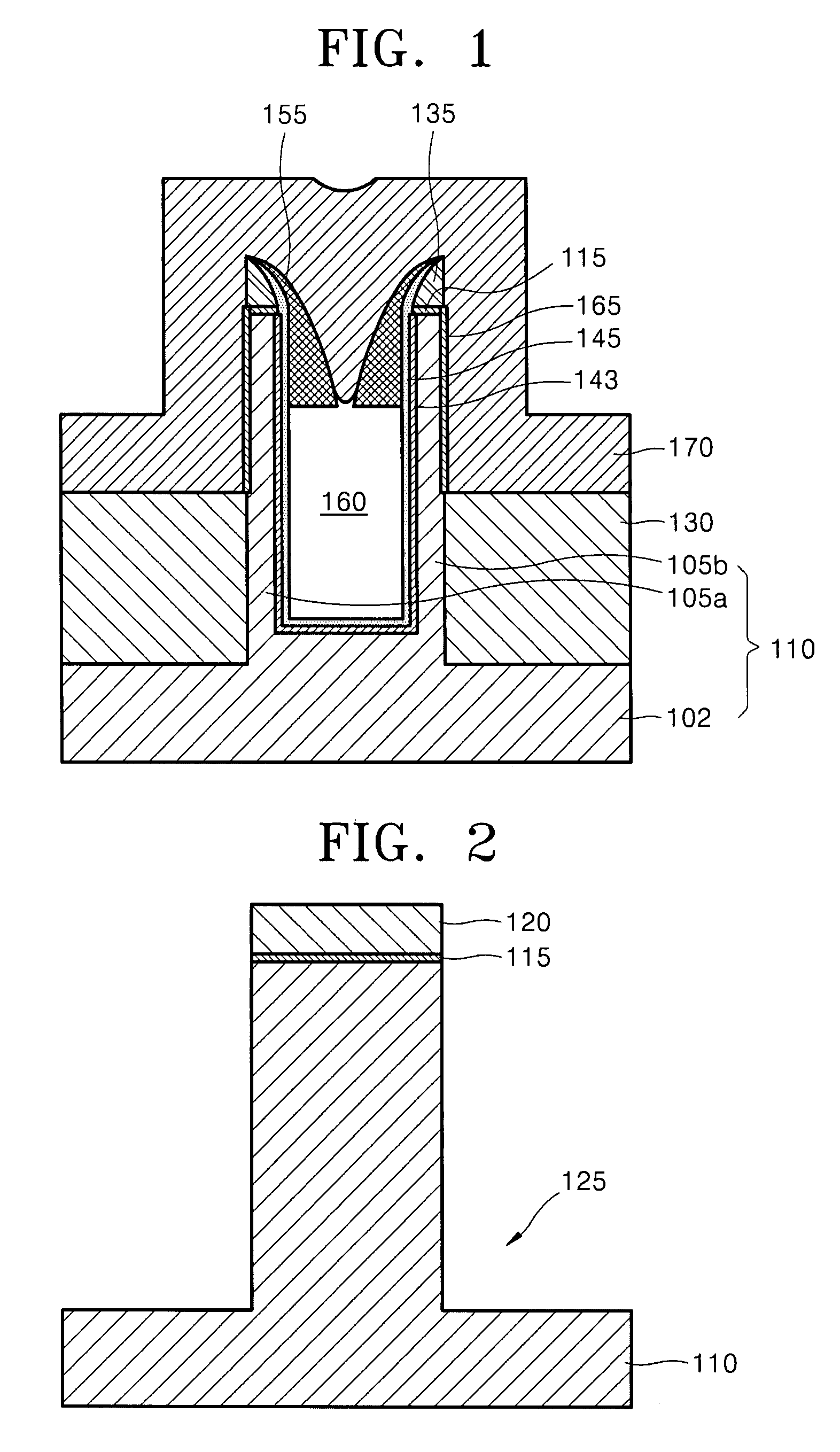
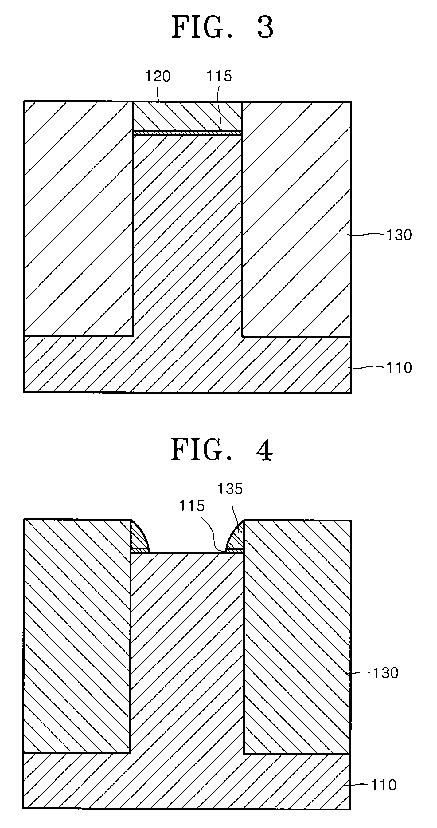
Example embodiments provide a non-volatile memory device with reduced disturbances during reading operations and a reduced short channel effect. The patent text describes a method of manufacturing a semiconductor device with a void between the pair of fins and a blocking insulating layer between the storage node layer and the gate electrode. The method includes etching the semiconductor substrate to form the body and the pair of fins, forming an inner spacer insulating layer on the inner sidewall of the fins, and forming a gate insulating layer on the outer sidewall of the fins. The void is defined by the blocking insulating layer. The technical effect of the patent text is to improve the performance and reliability of non-volatile memory devices.

Problems solved by technology

However, SOI substrates may be relatively expensive.
Furthermore, as the integration density of a semiconductor device increases, the distance between the fins may be reduced, thus resulting in disturbances during reading operations.

Method used


Image

  • Semiconductor device having a pair of fins and method of manufacturing the same
  • Semiconductor device having a pair of fins and method of manufacturing the same
  • Semiconductor device having a pair of fins and method of manufacturing the same

Examples


Embodiment Construction

[0016]Example embodiments will now be described more fully with reference to the accompanying drawings. Example embodiments may, however, be embodied in many different forms and should not be construed as being limited to the examples set forth herein. The sizes of elements in the drawings may have been exaggerated for purposes of illustration.

[0017]It will be understood that when an element or layer is referred to as being “on”, “connected to”, “coupled to”, or “covering” another element or layer, it may be directly on, connected to, coupled to, or covering the other element or layer or intervening elements or layers may be present. In contrast, when an element is referred to as being “directly on,”“directly connected to” or “directly coupled to” another element or layer, there are no intervening elements or layers present. Like numbers refer to like elements throughout. As used herein, the term “and / or” includes any and all combinations of one or more of the associated listed item...


PUM


Abstract

Example embodiments relate to a semiconductor device and a method of manufacturing the same. A semiconductor device according to example embodiments may have reduced disturbances during reading operations and a reduced short channel effect. The semiconductor device may include a semiconductor substrate having a body and a pair of fins protruding from the body. Inner spacer insulating layers may be formed on an upper portion of an inner sidewall of the pair of fins so as to reduce the entrance to the region between the pair of fins. A gate electrode may cover a portion of the external sidewalls of the pair of fins and may extend across the inner spacer insulating layers so as to define a void between the pair of fins. Gate insulating layers may be interposed between the gate electrode and the pair of fins.

Description

PRIORITY STATEMENT[0001]This application claims priority under 35 U.S.C. § 119 to Korean Patent Application No. 10-2006-0113043, filed on Nov. 15, 2006 and Korean patent application No. 10-2007-0094900 filed on Sep. 18, 2007, in the Korean Intellectual Property Office (KIPO), the entire contents of both of which are incorporated herein by reference.BACKGROUND[0002]1. Technical Field[0003]Example embodiments relate to a non-volatile memory device including a fin-type channel region and a method of manufacturing the non-volatile memory device.[0004]2. Description of the Related Art[0005]Along with further reductions in size, higher capacity data processing may be required for semiconductor products. Accordingly, increasing the operational speed and integration density of non-volatile memory devices used in semiconductor products may be beneficial. For example, a semiconductor device having a fin-FET structure may have a larger channel surface and, thus, may have increased operational ...

Claims


Application Information

Patent Timeline
Patent Type & Authority Patents(United States)
IPC IPC(8): H01L21/336
CPCH01L21/28273H01L21/28282H01L29/66795H01L29/792H01L29/66833H01L29/785H01L29/7881H01L29/66825H01L29/40114H01L29/40117
Inventor KIM, SUK-PILPARK, YOON-DONGLEE, JONG-JINKIM, WON-JOOKOO, JUNE-MOSONG, SEUNG-HWAN
Owner SAMSUNG ELECTRONICS CO LTD
Learn More