Semiconductor device having two fuses in parallel

a technology of fuses and circuits, applied in the field of circuits, can solve the problems of no breakdown connection in the electrical circuit, and may cause malfunction of operation, and achieve the effect of eliminating malfunction of operation

Inactive Publication Date: 2009-07-28
LONGITUDE SEMICON S A R L
View PDF18 Cites 12 Cited by
  • Summary
  • Abstract
  • Description
  • Claims
  • Application Information

AI Technical Summary

Benefits of technology

[0006]It is, therefore, an object of the present invention to provide a semiconductor device capable of substantially eliminating malfunction of operation which would be caused by process variations of an electric fuse portion.
[0009]According to the aspect of the present invention, the semiconductor device employs a plurality of electric fuses for an electric fuse portion. A predetermined output can be obtained if a breakdown connection is produced in any one of the electric fuses. Accordingly, malfunction of operation which would be caused by process variations of electric fuses can substantially be eliminated.

Problems solved by technology

However, even if the predetermined high voltage is applied to the electric fuse in the conventional semiconductor device, no breakdown connection may be produced in the electric fuse because of process variations thereof.
Accordingly, malfunction of operation may be caused in the conventional semiconductor device.

Method used


Image

  • Semiconductor device having two fuses in parallel
  • Semiconductor device having two fuses in parallel
  • Semiconductor device having two fuses in parallel

Examples


first embodiment

[0042]Referring to FIG. 3, a semiconductor device according to the present invention will be described below.

[0043]FIG. 3 is a circuit diagram showing an arrangement of an electric fuse portion (parallel electric fuse portion) 30 used in a storage device according to a first embodiment of the present invention. A main part of the storage device has the same arrangement as that of the conventional storage device shown in FIG. 1.

[0044]The electric fuse portion 30 shown in FIG. 3 differs from the conventional electric fuse portion 10 in that two electric fuses 31 and 32 are connected in parallel to each other. These electric fuses 31 and 32 are formed so as to have the same characteristics.

[0045]Operation of the electric fuse portion 30 shown in FIG. 3 is basically the same as that of the conventional electric fuse portion 10. However, there is a difference in breakdown connection of the electric fuses 31 and 32. This difference will be described below.

[0046]Since the electric fuses 31...

second embodiment

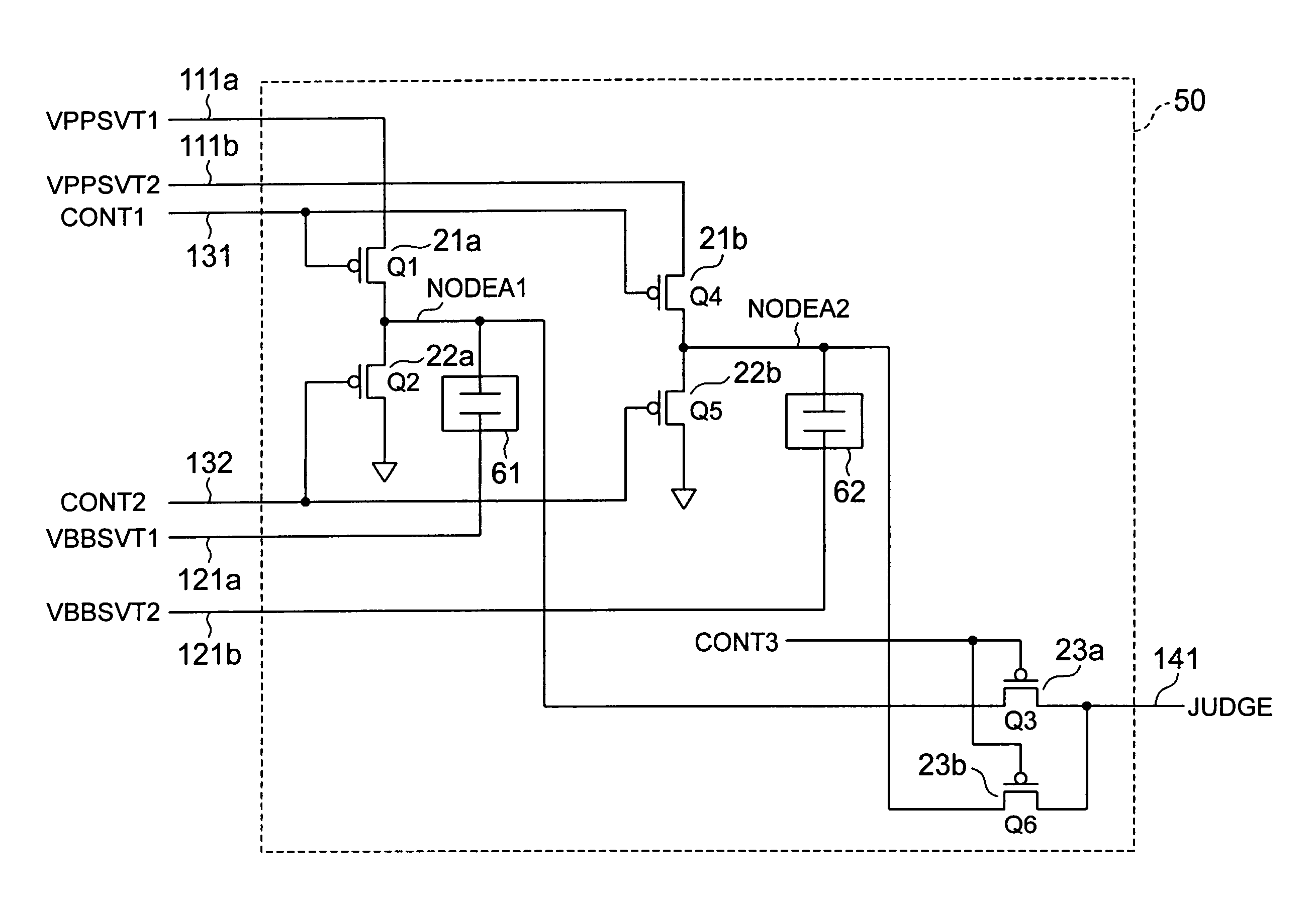
[0061]A storage device according to the present invention will be described with reference to FIGS. 5 and 6.

[0062]As shown in FIG. 5, the storage device in the present embodiment has two high voltage generation portions 11a and 11b and two low voltage generation portions 12a and 12b.

[0063]Each of the high voltage generation portions 11a and 11b has the same arrangement as the conventional high voltage generation portion 11. Similarly, each of the low voltage generation portions 12a and 12b has the same arrangement as the conventional low voltage generation portion 12.

[0064]The high voltage generation portions 11a and 11b are connected to an electric fuse portion (anti-parallel fuse portion) 50 via high potential application lines 111a and 111b, respectively. The low voltage generation portions 12a and 12b are connected to the electric fuse portion 50 via low potential application lines 121a and 121b, respectively.

[0065]The electric fuse portion 50 used in the storage device shown i...


PUM


Abstract

A semiconductor device employs two electric fuses (31, 32) connected in parallel to each other. First terminals of the electric fuses (31, 32) are connected to a junction of first and second P-channel transistors (21, 22), which are connected in series between a high potential application line (111) and a ground, and connected to a third P-channel transistor (23). Second terminals of the electric fuses (31, 32) are connected to a low potential application line (121). When an extra-high voltage is applied between the first and second terminals of the electric fuses (31, 32), a breakdown connection is produced in at least one of the electric fuses (31, 32). Thus, 1-bit information is written into the semiconductor device.

Description

[0001]This application claims priority to prior Japanese application JP 2005-308572, the disclosure of which is incorporated herein by reference.BACKGROUND OF THE INVENTION[0002]The present invention relates to a semiconductor device, and more particularly to a semiconductor device for storing information with use of a change of a state of an electric fuse employing a breakdown of an oxide film.[0003]A conventional semiconductor device has an electric fuse to store 1-bit information. The electric fuse is an element employing a breakdown of an oxide film. When the oxide film is in a normal state, the electric fuse has an extremely high resistance between terminals thereof. On the other hand, when the oxide film is broken down, the electric fuse has a relatively low resistance between the terminals. The breakdown of the oxide film is made by applying a predetermined high voltage between the terminals of the electric fuse. The conventional semiconductor device is configured so as to pr...

Claims


Application Information

Patent Timeline
Patent Type & Authority Patents(United States)
IPC IPC(8): H01H37/76H01H85/00
CPCG11C17/18G11C17/16
Inventor MATSUBARA, YASUSHI
Owner LONGITUDE SEMICON S A R L
Why Eureka
Try Eureka