Interconnect structure having enhanced electromigration reliability and a method of fabricating same

a technology of interconnect structure and reliability, which is applied in the direction of semiconductor devices, semiconductor/solid-state device details, electrical apparatus, etc., can solve the problems of circuit dead opening, worst reliability concerns of very large-scale integrated circuits, etc., to improve em reliability, prevent sudden data loss, and enhance the lifetime of semiconductor products

Inactive Publication Date: 2009-08-04
TAIWAN SEMICON MFG CO LTD
View PDF16 Cites 25 Cited by
  • Summary
  • Abstract
  • Description
  • Claims
  • Application Information

AI Technical Summary

Benefits of technology

[0009]In one aspect, the present invention relates to an interconnect structure having improved EM reliability. The inventive interconnect structure avoids a circuit dead opening that is caused by EM failure by incorporating an EM preventing liner within a metal interconnect. Other benefits of the inventive structure include: prevention of sudden data loss and enhancement of the lifetime of the semiconductor product.

Problems solved by technology

EM is one of the worst reliability concerns for very large scale integrated (VLSI) circuits.
The EM initial voids first nucleate at the metal / dielectric cap interface and then grow in the direction of the bottom of the interconnect, which eventually results in a circuit dead opening.

Method used


Image

  • Interconnect structure having enhanced electromigration reliability and a method of fabricating same
  • Interconnect structure having enhanced electromigration reliability and a method of fabricating same
  • Interconnect structure having enhanced electromigration reliability and a method of fabricating same

Examples


Embodiment Construction

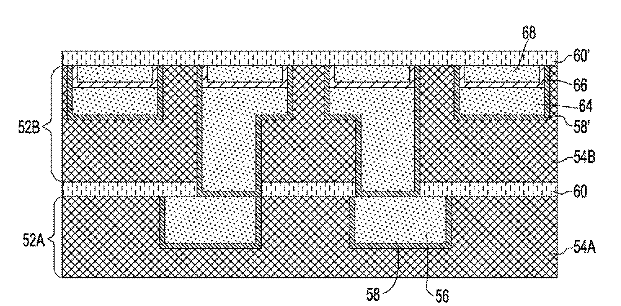
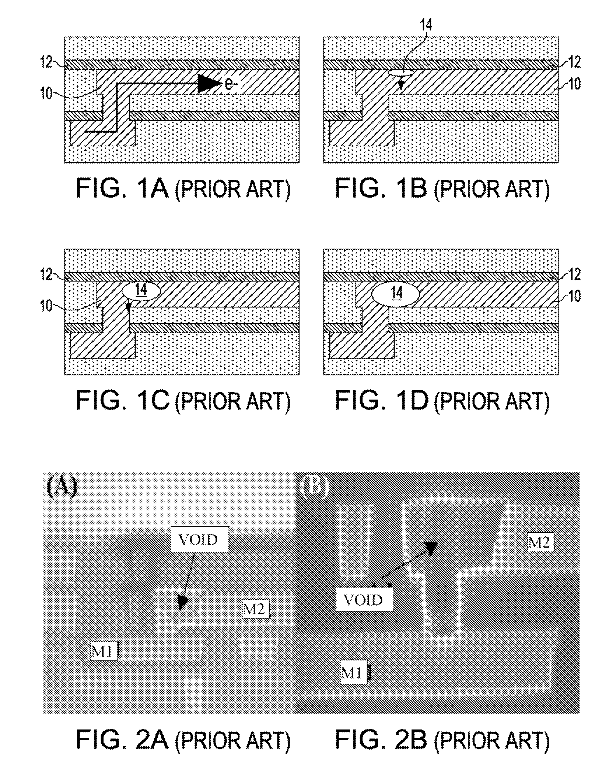
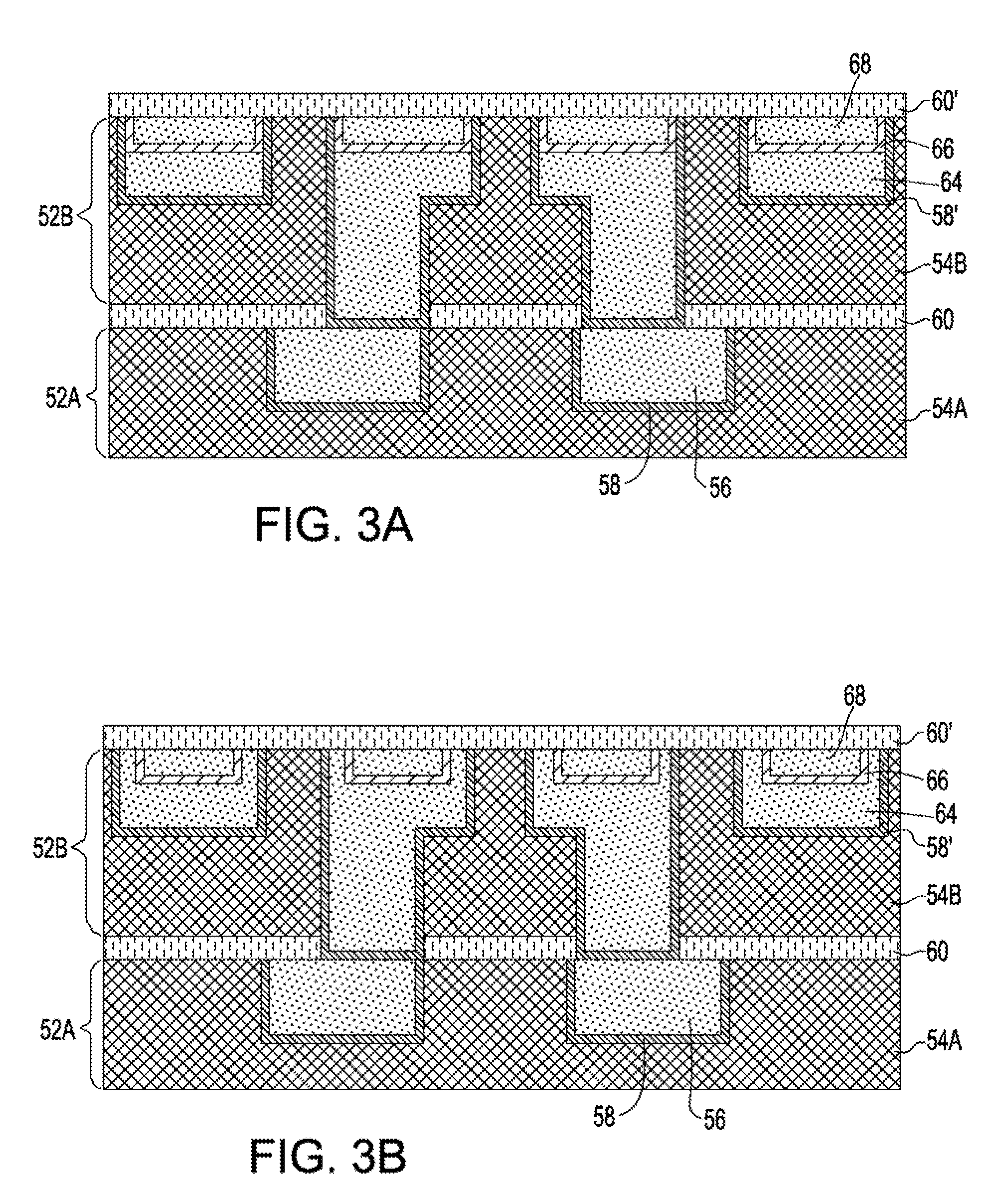
[0025]The present invention, which provides an interconnect structure having enhanced electromigration (EM) reliability and a method of forming the same, will now be described in greater detail by referring to the following discussion and drawings that accompany the present application. It is noted that the drawings of the present application are provided for illustrative purposes only and, as such, the drawings are not drawn to scale.

[0026]In the following description, numerous specific details are set forth, such as particular structures, components, materials, dimensions, processing steps and techniques, in order to provide a thorough understanding of the present invention. However, it will be appreciated by one of ordinary skill in the art that the invention may be practiced without these specific details. In other instances, well-known structure or processing steps have not been described in detail in order to avoid obscuring the invention.

[0027]It will be understood that when ...


PUM


Abstract

An interconnect structure having improved electromigration (EM) reliability is provided. The inventive interconnect structure avoids a circuit dead opening that is caused by EM failure by incorporating a EM preventing liner at least partially within a metal interconnect. In one embodiment, a “U-shaped” EM preventing liner is provided that abuts a diffusion barrier that separates conductive material from the dielectric material. In another embodiment, a space is located between the “U-shaped” EM preventing liner and the diffusion barrier. In yet another embodiment, a horizontal EM liner that abuts the diffusion barrier is provided. In yet a further embodiment, a space exists between the horizontal EM liner and the diffusion barrier.

Description

FIELD OF THE INVENTION[0001]The present invention relates to a semiconductor interconnect structure, and a method of fabricating the same. More particularly, the present invention relates to a semiconductor interconnect structure having enhanced electromigration (EM) reliability in which an EM preventing liner is present within a conductive feature of a dielectric material.BACKGROUND OF THE INVENTION[0002]Generally, semiconductor devices include a plurality of circuits which form an integrated circuit (IC) fabricated on a semiconductor substrate. A complex network of signal paths will normally be routed to connect the circuit elements distributed on the surface of the substrate. Efficient routing of these signals across the device requires formation of multilevel or multilayered schemes, such as, for example, single or dual damascene wiring structures. The wiring structure typically includes copper, Cu, since Cu based interconnects provide higher speed signal transmission between la...

Claims


Application Information

Patent Timeline
Patent Type & Authority Patents(United States)
IPC IPC(8): H01L21/4763
CPCH01L21/76847H01L23/5226H01L23/53295H01L23/53223H01L23/53238H01L23/5283H01L2924/0002H01L2924/00H01L21/28
Inventor YANG, CHIH-CHAOWANG, PING-CHUANWANG, YUN-YU
Owner TAIWAN SEMICON MFG CO LTD
Why Eureka
Try Eureka