Discontinuous/non-uniform metal cap structure and process for interconnect integration

a metal cap and interconnect technology, applied in the direction of semiconductor devices, semiconductor/solid-state device details, electrical apparatus, etc., can solve the problems of process cost, electrical short circuit between adjacent interconnects, and dead opening of circuits, so as to improve reliability, improve reliability, and improve the effect of em reliability

Active Publication Date: 2010-04-08
IBM CORP
View PDF30 Cites 11 Cited by
  • Summary
  • Abstract
  • Description
  • Claims
  • Application Information

AI Technical Summary

Benefits of technology

[0012]The present invention provides semiconductor interconnect structures that have improved EM reliability. The improved EM reliability is obtained without degrading the time dependent dielectric breakdown reliability of the interconnect structures. The present invention further provides interconnect structures that have better reliability and technology extendibility for the semiconductor industry.

Problems solved by technology

The EM initial voids first nucleate at the metal / dielectric cap interface and then grow in the direction to the bottom of the interconnect, which eventually results in a circuit dead opening.
One problem with utilizing such selective deposited metal caps is that some of the metal cap extends onto the adjoining surface of the interconnect dielectric material and, as such, electrical shorts between adjacent interconnects may arise.
Although this prior art recess process provides a metal cap that is located only on a surface of the recessed conductive material, such a process is problematic since there is high process cost associated therewith.
It is also worth mentioning that during a clean in dilute hydrofluoric acid, which is generally used to clean the surface of the interconnect dielectric material, corrosion of metal caps may occur.

Method used


Image

  • Discontinuous/non-uniform metal cap structure and process for interconnect integration
  • Discontinuous/non-uniform metal cap structure and process for interconnect integration
  • Discontinuous/non-uniform metal cap structure and process for interconnect integration

Examples


Embodiment Construction

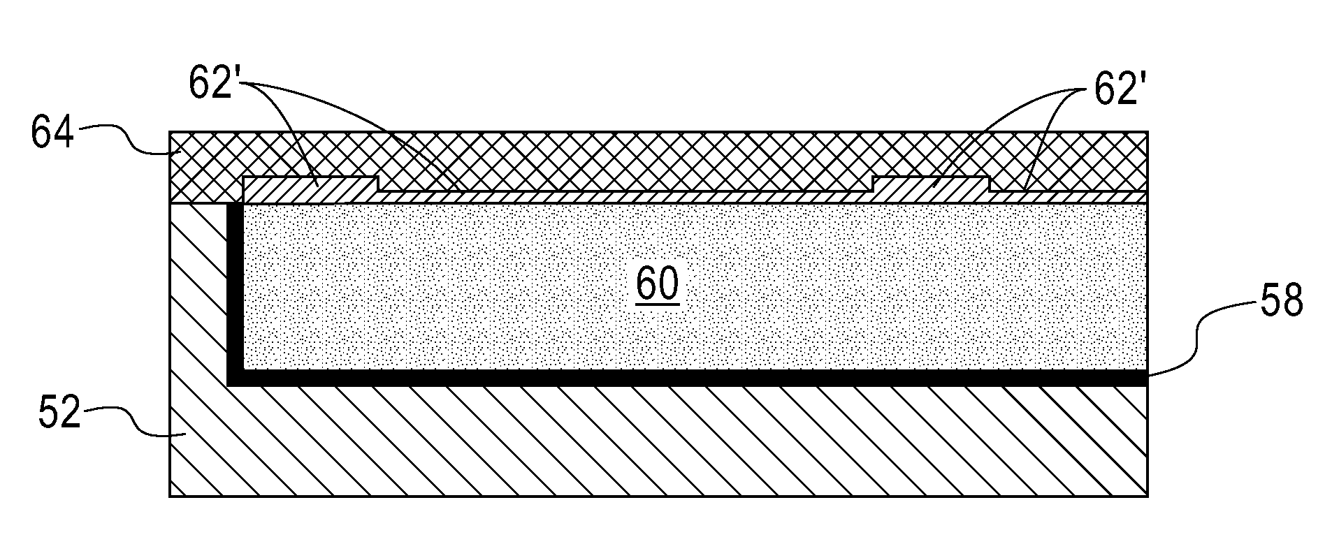
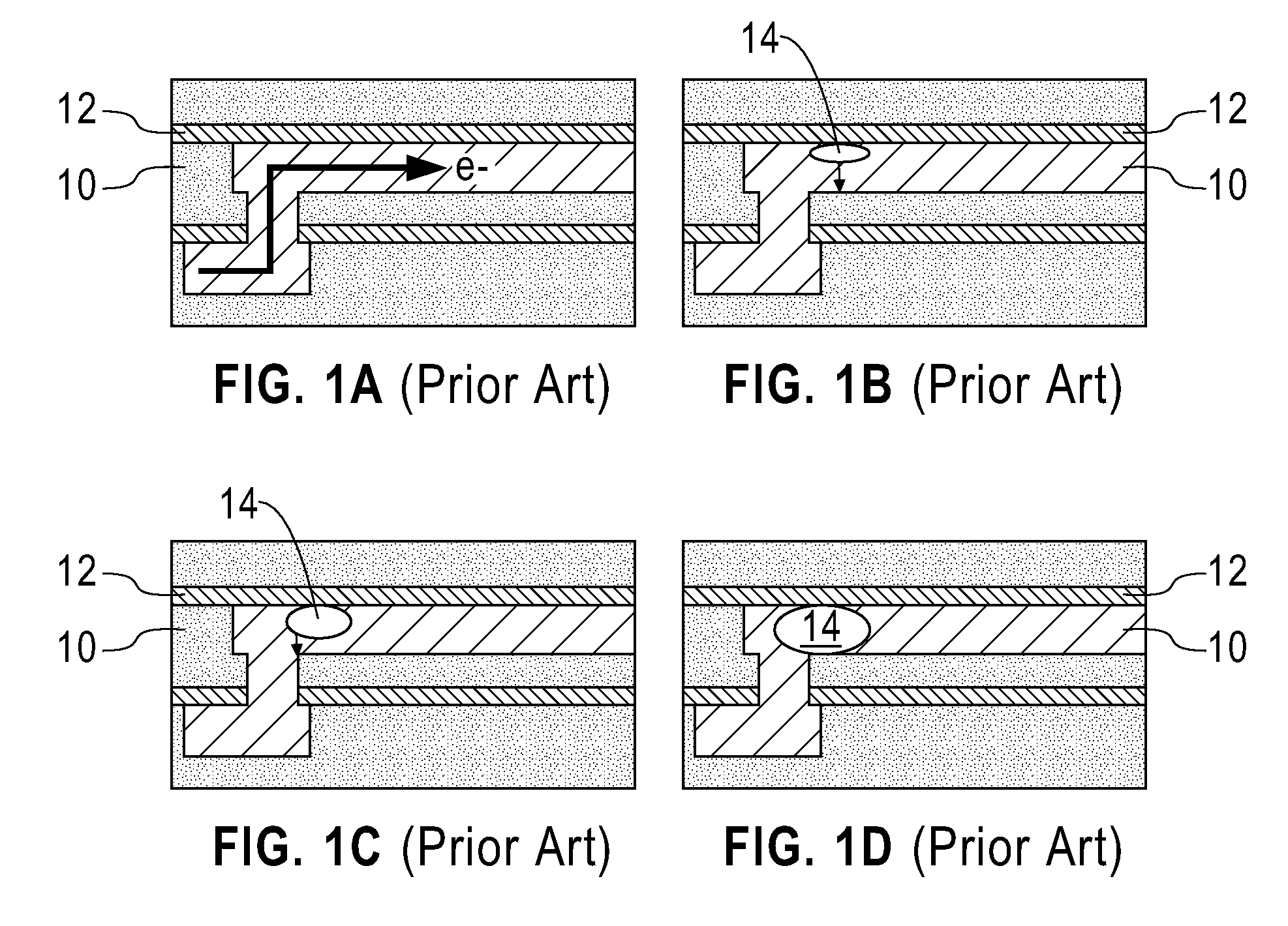
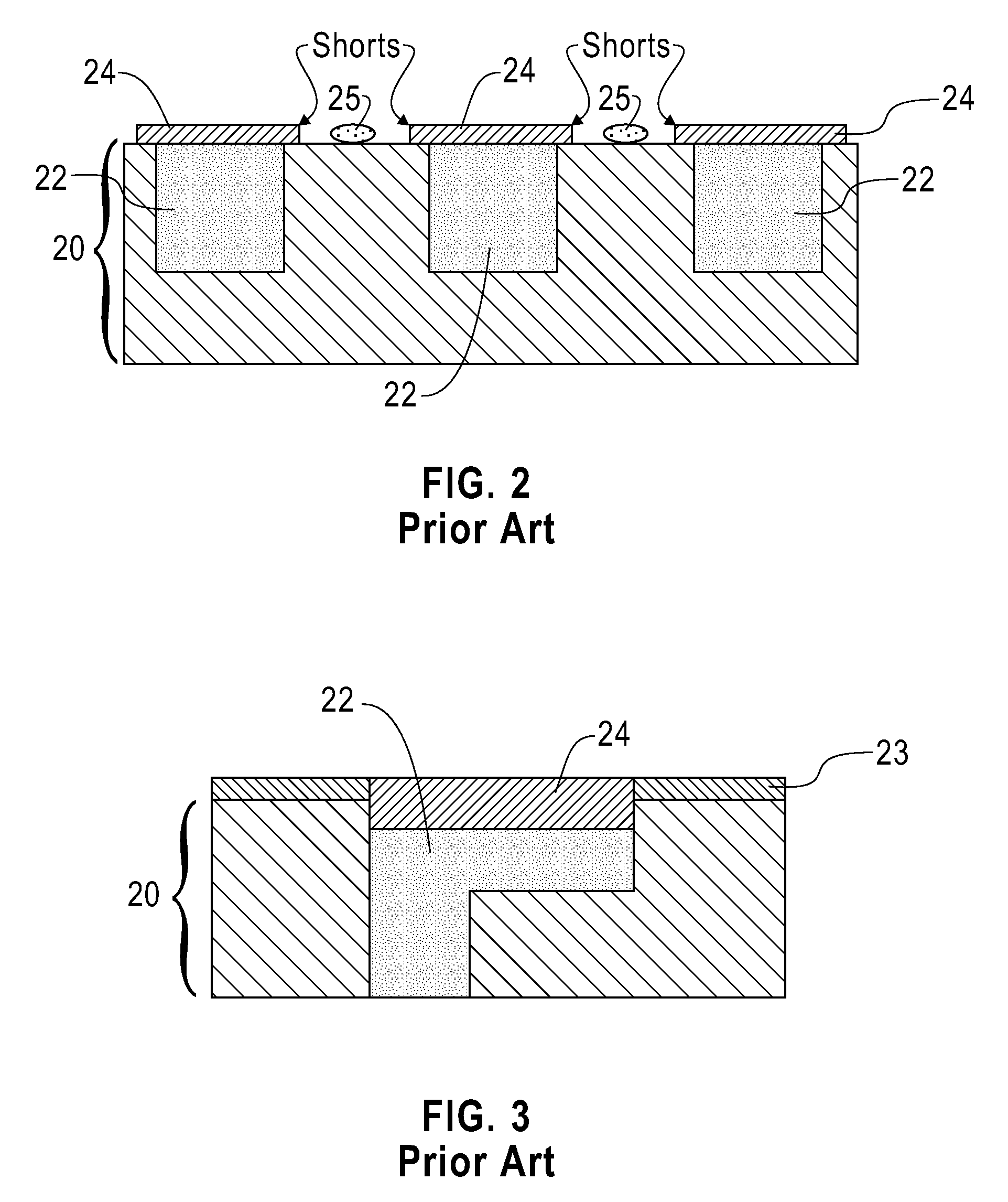
[0033]The present invention, which provides interconnect structures having enhanced electromigration (EM) resistance without degrading time dependent dielectric breakdown reliability and a method of forming the same, will now be described in greater detail by referring to the following discussion and drawings that accompany the present application. It is noted that the drawings of the present application are provided for illustrative purposes only and, as such, the drawings are not drawn to scale.

[0034]In the following description, numerous specific details are set forth, such as particular structures, components, materials, dimensions, processing steps and techniques, in order to provide a thorough understanding of the present invention. However, it will be appreciated by one of ordinary skill in the art that the invention may be practiced without these specific details. In other instances, well-known structures or processing steps have not been described in detail in order to avoi...


PUM

PropertyMeasurementUnit
dielectric constantaaaaaaaaaa
temperatureaaaaaaaaaa
pressureaaaaaaaaaa

Abstract

An interconnect structure including a noble metal-containing cap that is present at least on some portion of an upper surface of at least one conductive material that is embedded within an interconnect dielectric material is provided. In one embodiment, the noble metal-containing cap is discontinuous, e.g., exists as nuclei or islands on the surface of the at least one conductive material. In another embodiment, the noble metal-containing cap has a non-uniform thickness across the surface of the at least one conductive material.

Description

FIELD OF THE INVENTION[0001]The present invention relates to semiconductor interconnect structures, and a method of fabricating the same. More particularly, the present invention relates to semiconductor interconnect structures having enhanced electromigration (EM) resistance without degrading time dependent dielectric breakdown reliability.BACKGROUND OF THE INVENTION[0002]Generally, semiconductor devices include a plurality of circuits that form an integrated circuit (IC) fabricated on a semiconductor substrate. A complex network of signal paths will normally be routed to connect the circuit elements distributed on the surface of the substrate. Efficient routing of these signals across the device requires formation of multilevel or multilayered schemes, such as, for example, single or dual damascene wiring structures. The wiring structure typically includes copper, Cu, since Cu based interconnects provide higher speed signal transmission between large numbers of transistors on a co...

Claims


Application Information

Patent Timeline
Patent Type & Authority Applications(United States)
IPC IPC(8): H01L23/52H01L21/4763
CPCH01L21/76849H01L21/76868H01L23/5283H01L23/53223H01L23/53238H01L23/53266H01L23/53252H01L2924/0002H01L23/5329H01L21/76865H01L21/02362H01L2924/00H01L21/28H01L21/768
Inventor YANG, CHIH-CHAOGIGNAC, LYNNE M.HU, CHAO-KUNMITTAL, SURBHI
Owner IBM CORP
Why Eureka
Try Eureka