In-plane switching mode liquid crystal display device
a liquid crystal display and switching mode technology, applied in non-linear optics, instruments, optics, etc., can solve the problems of affecting the picture quality of liquid crystal panels. , to achieve the effect of enhancing the picture quality of the liquid crystal panel and preventing the degradation of picture quality
- Summary
- Abstract
- Description
- Claims
- Application Information
AI Technical Summary
Benefits of technology
Problems solved by technology
Method used
Image
Examples
first embodiment
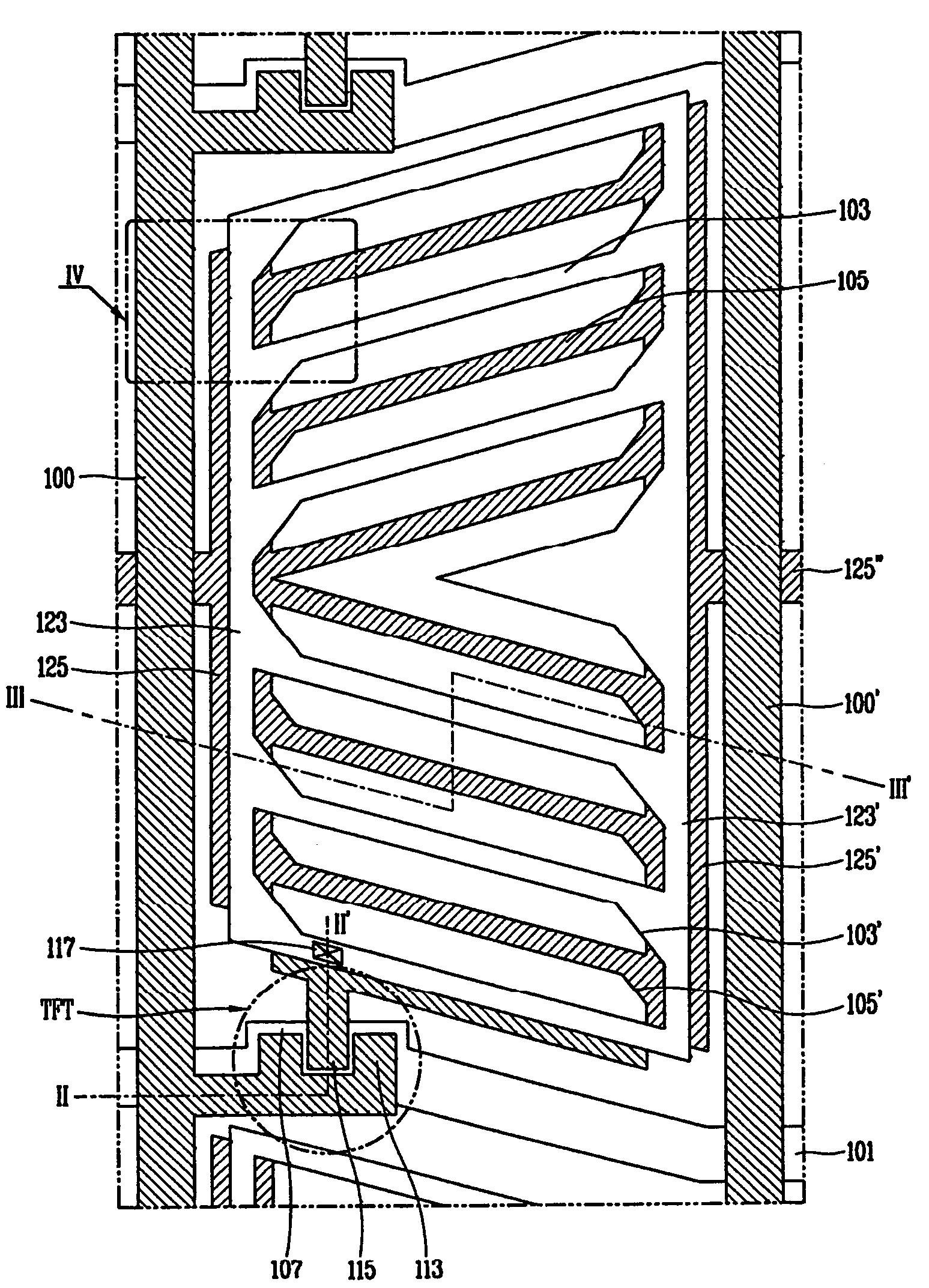
[0039]FIG. 3 shows an exemplary pixel region of an LCD device in accordance with the present invention. FIG. 4A is a cross-sectional view taken along line II-II′ of FIG. 3. FIG. 4B is a cross-sectional view taken along line III-III′ of FIG. 3. Referring to FIGS. 3, 4A and 4B, a liquid crystal panel includes a data line 100 and a gate line 101 arranged on a first substrate 110 and defining a pixel region, a switching device, such as a thin film transistor TFT, disposed at the crossing of the gate line 101 and the data line 100, and at least one pixel electrode 103 and one common electrode 105 alternately arranged in parallel to each other in the pixel region to generate a horizontal electric field. An alignment film (not shown) is formed on the first substrate 110 including the pixel electrode 103 and the common electrode 105. The alignment film is rubbed in the direction perpendicular to the data line 100. The pixel electrode 103 and the common electrode 105 are formed to have a til...
second embodiment
[0049]However, a vertical dim phenomenon may occur in the LCD device due to a parasitic capacitance between the data line 100 and the pixel electrode 103. the present invention is directed to an IPS mode LCD capable of enhancing picture quality of the liquid crystal panel, especially by removing the vertical line phenomenon.
[0050]FIG. 5 shows an exemplary pixel region of an LCD device in accordance with a second embodiment of the present invention. The structure of the second embodiment of the present invention is similar to that of the first embodiment, so only different portions of the second embodiment will be described in further details. The same reference numerals in FIG. 5 refer to the same or like elements of the LCD device of FIG. 3. In the second embodiment of the present invention, the second pixel electrode line 123′ (shown in FIG. 3) has been removed.
[0051]Referring to FIG. 5, a liquid crystal panel includes a data line 200 and a gate line 201 arranged on a first substr...
PUM
| Property | Measurement | Unit |
|---|---|---|
| isolation distance | aaaaa | aaaaa |
| frequency | aaaaa | aaaaa |
| frequency | aaaaa | aaaaa |
Abstract
Description
Claims
Application Information


