Supercharge Your Innovation With Domain-Expert AI Agents!

Method of programming multi-level semiconductor memory device and multi-level semiconductor memory device

a memory device and multi-level technology, applied in the field of programming methods and semiconductor memory devices, can solve problems such as data write speed slowdown

Active Publication Date: 2009-08-18
SAMSUNG ELECTRONICS CO LTD
View PDF1 Cites 0 Cited by
  • Summary
  • Abstract
  • Description
  • Claims
  • Application Information

AI Technical Summary

Benefits of technology

Example embodiments provide a method and device for programming a memory cell using three latches. The method involves storing data bits in a first latch, then transferring them to a second latch, and finally writing them to a memory cell using a reference to the data stored in the first latch. This allows for faster programming of memory cells and reduces the likelihood of errors. The device includes a memory cell, three latches, and a logic circuit to facilitate the programming process. The technical effect is improved programming speed and reliability in semiconductor memory devices.

Problems solved by technology

However, if the data storage state of the second bit is read from the memory cell during a data write operation, a data write speed slows down.

Method used


Image

  • Method of programming multi-level semiconductor memory device and multi-level semiconductor memory device
  • Method of programming multi-level semiconductor memory device and multi-level semiconductor memory device
  • Method of programming multi-level semiconductor memory device and multi-level semiconductor memory device

Examples


Embodiment Construction

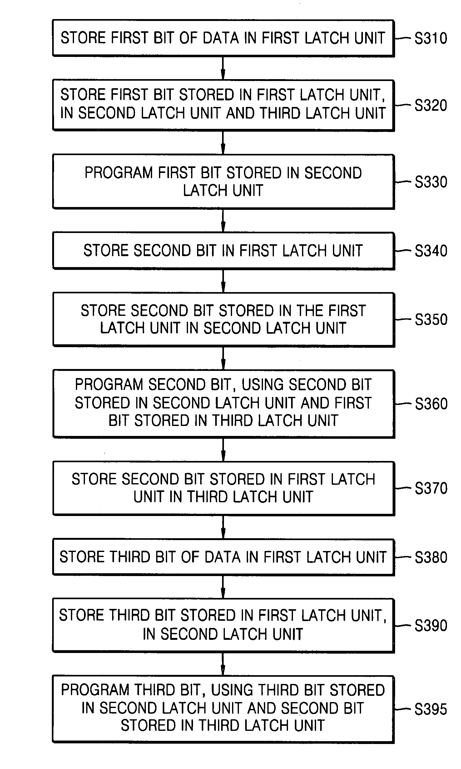
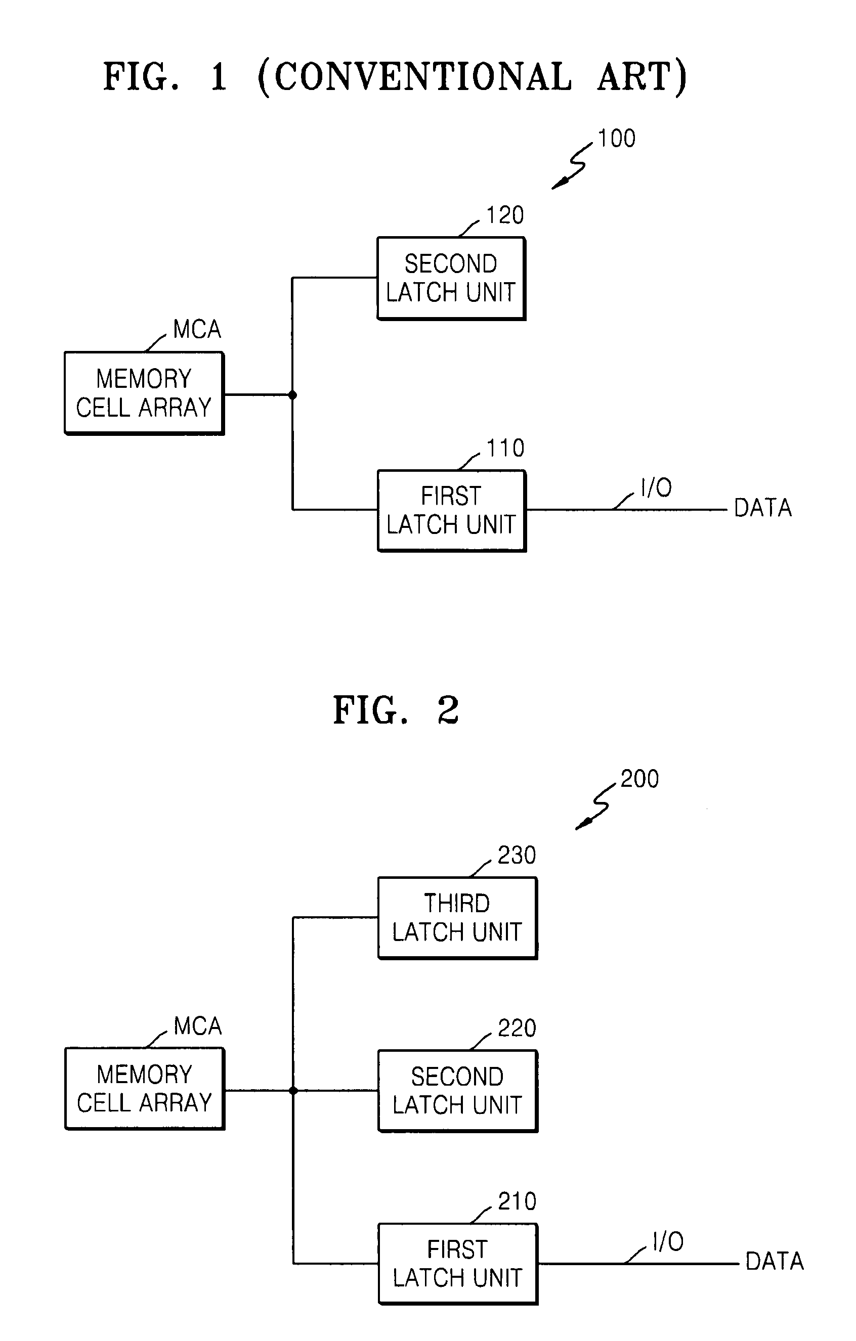
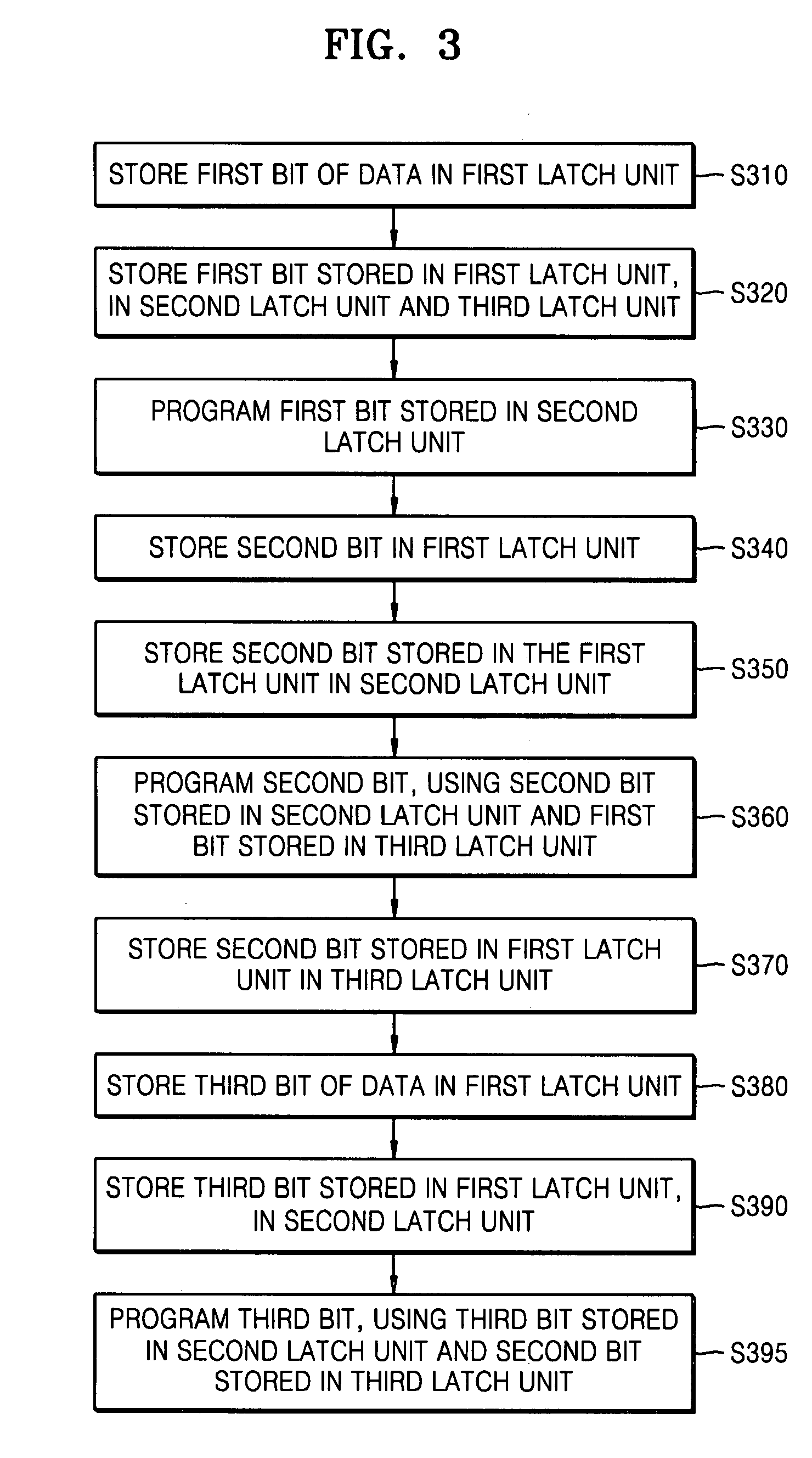
[0023]The attached drawings are referred to in order to gain an understanding of example embodiments.

[0024]It will be understood that, although the terms first, second, third etc. may be used herein to describe various elements, components, regions, layers and / or sections, these elements, components, regions, layers and / or sections should not be limited by these terms. These terms may be only used to distinguish one element, component, region, layer or section from another region, layer or section. Thus, a first element, component, region, layer or section discussed below could be termed a second element, component, region, layer or section without departing from the teachings of the present invention.

[0025]The terminology used herein is for the purpose of describing particular example embodiments only and is not intended to be limiting. As used herein, the singular forms “a”, “an” and “the” may be intended to include the plural forms as well, unless the context clearly indicates ot...


PUM


Abstract

Provided in one example embodiment, a method of programming n bits of data to a semiconductor memory device may include outputting a first bit of data written in a memory cell from a first latch, storing the first bit of the data to a third latch, storing a second bit of the data to the first latch, outputting the second bit of the data from the first latch, storing the second bit of the data to the second latch, and writing the second bit of the data stored in the second latch to the memory cell with reference to a data storage state of the first bit of the data stored in the third latch.

Description

PRIORITY CLAIM[0001]A claim of priority is made to Korean Patent Application No. 10-2006-0136821, filed on Dec. 28, 2006, in the Korean Intellectual Property Office, the disclosure of which is incorporated herein in its entirety by reference.BACKGROUND[0002]1. Field[0003]Example embodiments of the present invention may relate to a programming method and a semiconductor memory device, and more particularly, to a method of programming a multi-level semiconductor memory device and a multi-level semiconductor memory device.[0004]2. Description of the Related Art[0005]A non-volatile memory device may electrically erase and program data, and may retain stored data even if power is not applied thereto. A representative non-volatile memory device is a flash memory device.[0006]Each memory cell of a flash memory device includes a cell transistor having a control gate, a floating gate, and source and drain regions. The cell transistor programs and erases by a Fowler-Nordheim (F-N) tunneling.[...

Claims


Application Information

Patent Timeline
Patent Type & Authority Patents(United States)
IPC IPC(8): G11C7/00
CPCG11C11/5628G11C16/10G11C2211/5642G11C16/06
Inventor HYUN, JAE-WOONGCHO, KYOUNG-LAEPARK, KYU-CHARNPARK, YOON-DONGLEE, CHOONG-HOBYUN, SUNG-JAE
Owner SAMSUNG ELECTRONICS CO LTD
Features
  • R&D
  • Intellectual Property
  • Life Sciences
  • Materials
  • Tech Scout
  • Unparalleled Data Quality
  • Higher Quality Content
  • 60% Fewer Hallucinations
Learn More