Dielectric ceramic composition and electronic device

a technology of ceramic composition and electronic device, which is applied in the direction of fixed capacitors, electrical equipment, basic electric elements, etc., can solve the problems of lowering reliability and more significant problems, and achieve the effects of less electrostriction, accelerated lifetime of insulation resistance, and improved withstand pressure (breakdown voltage)

Active Publication Date: 2009-08-25
TDK CORPARATION
View PDF10 Cites 11 Cited by
  • Summary
  • Abstract
  • Description
  • Claims
  • Application Information

AI Technical Summary

Benefits of technology

[0010]A purpose of the present invention, reflecting this situation, is to provide a dielectric ceramic composition, able to be fired in a reducing atmosphere, less in electrostriction when applying a voltage and able to improve withstand pressure (breakdown voltage) and accelerated lifetime of insulation resistance as well as maintaining good specific permittivity and capacitance-temperature characteristics, and an electronic device comprising the dielectric ceramic composition as a dielectric layer.
[0038]Because a dielectric ceramic composition of the present invention comprises the above-described specified composition, it is able to be fired in a reducing atmosphere, less in electrostriction when applying a voltage and able to improve withstand pressure and accelerated lifetime of insulation resistance as well as maintaining good specific permittivity and capacitance-temperature characteristics. Especially, in the present invention, a ratio of BanZrO2+n is relatively high, i.e. 35 to 65 moles and preferably 40 to 55 moles with respect to 100 moles of BamTiO2+m, which allows to provide a dielectric ceramic composition with improved capacitance-temperature characteristics and withstand pressure.
[0039]Therefore, by adopting the dielectric ceramic composition of the present invention in a dielectric layer of an electronic device such as a multilayer ceramic capacitor, for example, when making the dielectric layer as thin as 20 μm and using the electronic device in mid-high voltage applications with high rated voltage (e.g. 100V or more, especially 250V or more), it is possible to attain high reliability. Namely, there is provided a highly-reliable electronic device for mid-high voltage applications, able to be downsized and increase capacitance.

Problems solved by technology

However, a dielectric ceramic composition according to the Japanese Patent Publication 3567759 is low in withstand pressure (breakdown voltage) and insufficient in lifetime characteristics (accelerated lifetime of insulation resistance), resulting in a problem of lowering reliability.
Especially, the problem is more significant when downsizing and increasing capacitance of a multilayer ceramic capacitor.

Method used


Image

  • Dielectric ceramic composition and electronic device
  • Dielectric ceramic composition and electronic device

Examples


first embodiment

Multilayer Ceramic Capacitor 1

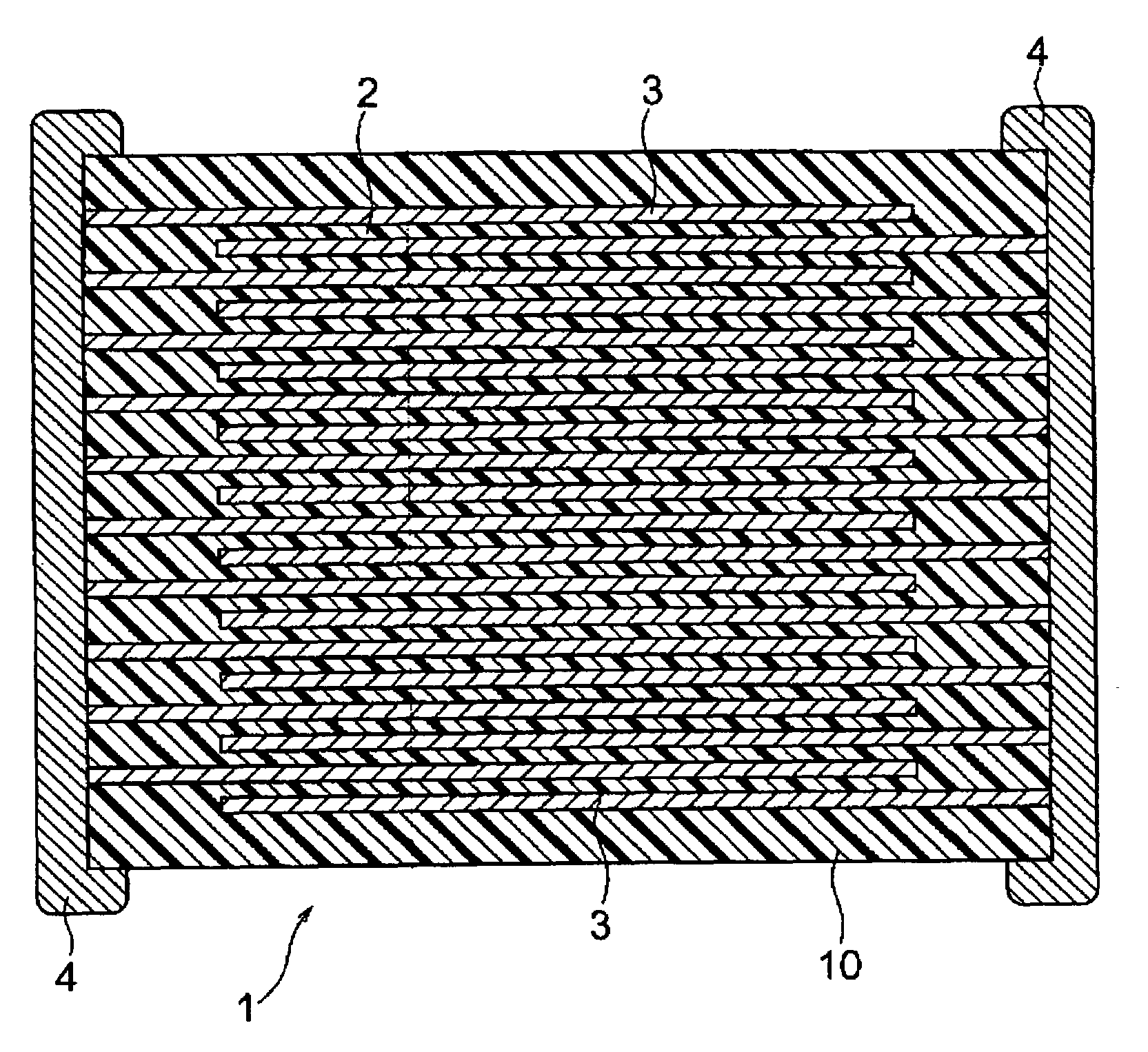
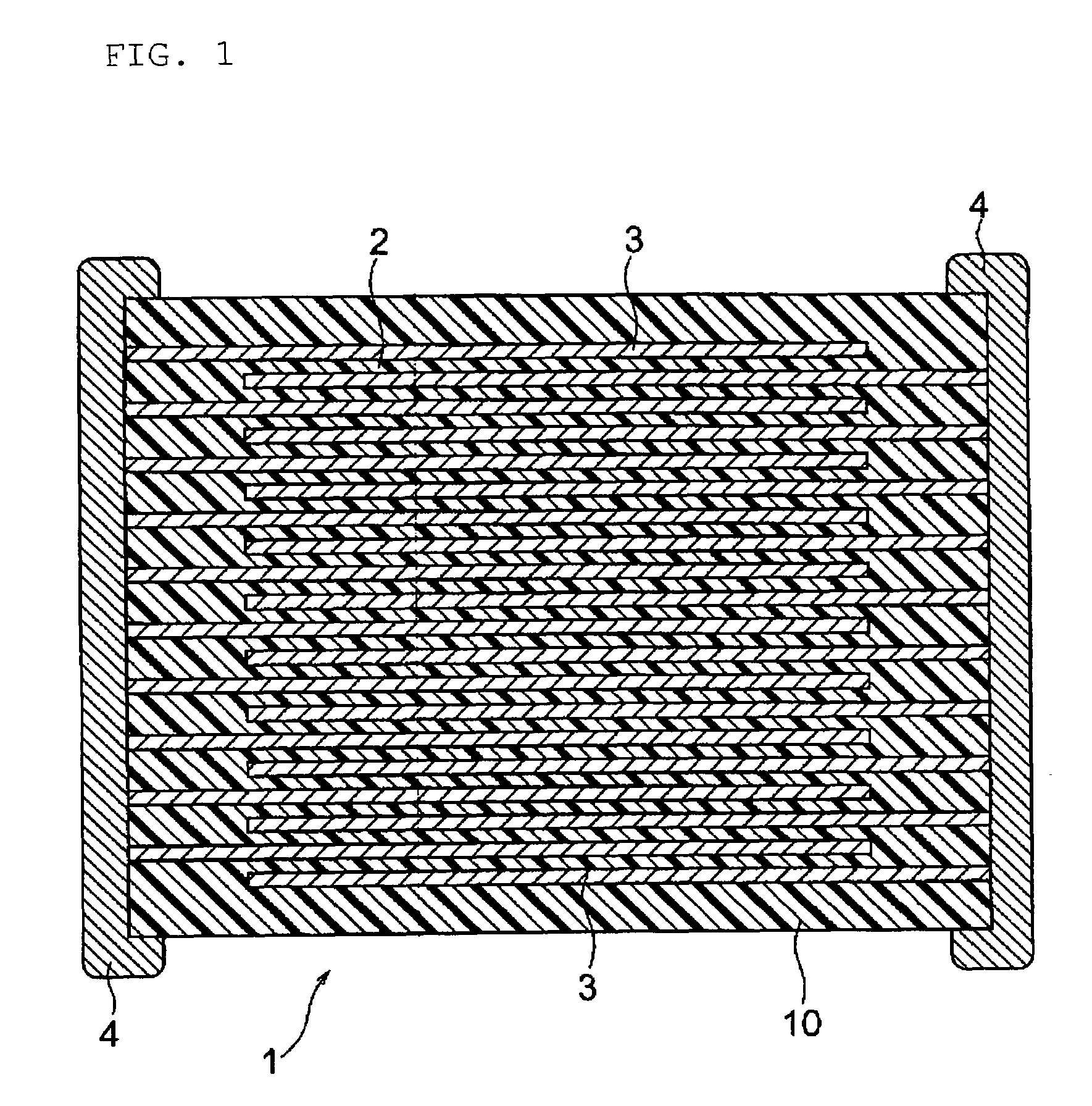
[0043]As shown in FIG. 1, a multilayer ceramic capacitor 1 according to an embodiment of the present invention comprises a capacitor device body 10 wherein a dielectric layer 2 and an internal electrode layer 3 are alternately stacked. At the both end portions of the capacitor device body 10, a pair of external electrodes 4, connected with internal electrode layers 3 alternately stacked inside the device body 10, is formed. The shape of the capacitor device body 10 is not particularly limited, and is normally rectangular parallelepiped. Also, its dimension is not particularly limited, and may be properly changed as usage.

[0044]The internal electrode layers 3 are stacked so that each end face is alternately exposed to a surface of the two opposed end portions of the capacitor device body 10. The pair of external electrodes 4 is formed at both end portions of the capacitor device body 10, and connected with the exposed end faces of the alternately-stacked...

second embodiment

[0090]A multilayer ceramic capacitor according to the second embodiment of the present invention and a production method thereof are same in the compositions of the dielectric ceramic composition and its production method as the dielectric ceramic composition according to the first embodiment, except for the following points, and explanation of the overlapped contents will be eliminated.

[0091]The dielectric ceramic composition according to the second embodiment comprises:

[0092]a first component expressed by a formula (BaaRb)α(TicZrdMge)O3,

[0093]a second component comprised of an oxide of at least one element selected from Mn, Cr, Co and Fe, and

[0094]a third component comprised of an oxide of at least one element selected from Si, Li, Al, Ge and B. In the above formula, R is rare-earth element as with the first embodiment, and is preferably Gd.

[0095]In the above formula,

[0096]0.8≦a≦0.96, preferably 0.83≦a≦0.93 and further preferably 0.86≦a≦0.91;

[0097]0.04≦b≦0.2, preferably 0.08≦b≦0.1...

example 1

[0115]At first, BamTiO2+m with an average particle size of 0.5 μm, BanZrO2+n, MgCO3, Gd2O3, MnO, and SiO2 were prepared and mixed by a ball mill. The obtained mixture of the powders was preliminarily calcined at 1200° C. to obtain calcined powders with an average particle size of 0.6 μm. Then, the obtained calcined powders were wet pulverized by a ball mill for 15 hours, and then dried to obtain a dielectric material. Note that MgCO3 became MgO in the dielectric ceramic composition after firing. Also, the state of the powders are not limited, and for example, BanZrO2+n, MgCO3, Gd2O3, MnO and SiO2 may be solid-dissolved within BamTiO2+m, MgCO3, Gd2O3, MnO and SiO2 may be diffused in the surface of BamTiO2+m, or MgCO3 particles, Gd2O3 particles, MnO particles and SiO2 particles may be firmly fixed on the surface of BamTiO2+m. The powder produced by this method was defined as powder “A”.

[0116]The amount of each component is shown in Table 1. In the present example, as shown in Table 1,...


PUM

PropertyMeasurementUnit
rated voltageaaaaaaaaaa
particle sizeaaaaaaaaaa

Abstract

The invention aims at providing a dielectric ceramic composition including BamTiO2+m where “m” satisfies 0.99≦m≦1.01 and BanZrO2+n where “n” satisfies 0.99≦n≦1.01, an oxide of Mg, an oxide of R where R is at least one selected from Sc, Y, La, Ce, Pr, Nd, Pm, Sm, Eu, Gd, Tb, Dy, Ho, Er, Tm, Yb and Lu, an oxide of at least one element selected from Mn, Cr, Co and Fe, and an oxide of at least one element selected from Si, Li, Al, Ge and B. 35 to 65 moles of BanZrO2+n, 4 to 12 moles of an oxide of Mg, 4 to 15 moles of an oxide of R, 0.5 to 3 moles of an oxide of Mn, Cr, Co and Fe, and 3 to 9 moles of an oxide of Si, Li, Al, Ge and B are included therein per 100 moles of the BamTiO2+m.

Description

BACKGROUND OF THE INVENTION[0001]1. Field of the Invention[0002]The present invention relates to a dielectric ceramic composition having resistance to reduction and an electronic device comprising the dielectric ceramic composition in a dielectric layer, and further specifically, relates to a dielectric ceramic composition with high rated voltage (e.g. 100V or more), preferable to use in mid-high voltage applications, and electronic device.[0003]2. Description of the Related Art[0004]A multilayer ceramic capacitor, an example of electronic devices, for example, is manufactured by firing a green chip obtained by stacking alternately ceramic green sheets comprising pre-determined dielectric ceramic composition and internal electrode layers in a pre-determined pattern to be integrated. Since the internal electrode layer of multilayer ceramic capacitor is integrated with the ceramic dielectric body by firing, a material not reacted with the ceramic dielectric body needs to be selected. ...

Claims


Application Information

Patent Timeline
Patent Type & Authority Patents(United States)
IPC IPC(8): H01G4/06
CPCC04B35/49H01G4/30C04B35/638H01G4/1227C04B35/62685C04B2235/3203C04B2235/3206C04B2235/3215C04B2235/3217C04B2235/3224C04B2235/3225C04B2235/3227C04B2235/3229C04B2235/3236C04B2235/3241C04B2235/3248C04B2235/3262C04B2235/3272C04B2235/3277C04B2235/3279C04B2235/3287C04B2235/3409C04B2235/3418C04B2235/5445C04B2235/6025C04B2235/6562C04B2235/6565C04B2235/6567C04B2235/6582C04B2235/6584C04B2235/6588C04B2235/663C04B2235/768C04B2235/79
Inventor AMAN, SANSHIROKOJIMA, TAKASHIMIYAUCHI, MARIHOSONO, MASAKAZUSAKURAI, DANTAKANO, KOSUKEMORIGASAKI, NOBUTO
Owner TDK CORPARATION
Why Eureka
Try Eureka