Method and related apparatus for calibrating signal driving parameters between chips

a signal driving and chip technology, applied in error detection/correction, bulk negative resistance effect devices, instruments, etc., can solve the problem that the force of the master chip cannot correctly pull up the electronic level, and achieve the effect of smooth laptop function

Active Publication Date: 2009-09-08
VIA TECH INC
View PDF3 Cites 16 Cited by
  • Summary
  • Abstract
  • Description
  • Claims
  • Application Information

AI Technical Summary

Benefits of technology

[0009]In an embodiment of the present invention, before two chips A and B, which are coupled to each other, can co-operate with each other, chip A and chip B first perform a cross-test of driving force. That is, a chip (e.g. chip A) is utilized as a master, and the other chip (chip B) is utilized as a slave. The master chip starts to output different test signals by using different driving forces in order to represent a same test value. After the slave chip receives the test signal, the slave chip can read the signals one by one and respond by sending a value to the master chip. This allows the master chip to compare the value with the test value and to determine which driving force is better.
[0012]In the prior art, each chip switches data / signals with other chips according to predetermined driving forces / reference values. However, the environment the chips operate in (including the impedances of the circuit board, temperatures, and the operations of another chip) can often cause some problems when the chip operates. Therefore, if each chip can only utilize the embedded predetermined driving forces / reference values to output or read signals, the chip cannot dynamically support different environments. In contrast to the prior art, the present invention performs tests before the chips operate and exchange data / signals such that the acceptable driving forces / reference values can be detected first. Therefore, the chip can be ensured to dynamically support all kinds of operational environments. In other words, the present invention chips can correctly exchange signals / data in different operational environments.
[0013]The present invention may be utilized in a laptop. Because the space demand of the laptop is strict, the system designer of the laptop may need to place chips in a special arrangement. For example, the signal wire of a particular chip may need to cross different layers of the circuit board or other devices such that the particular chip can be connected to another chip. Furthermore, laptops are often utilized in different environments (both outdoors and indoors). Due to the above-mentioned factors, each chip of the laptop often needs to operate in a difficult environment. Therefore, when the present invention is implemented in the laptop, tests between chips can be performed before the laptop is booted. This can ensure that each chip of the laptop can correctly exchange signals / data such that the whole function of the laptop can be smoothly achieved.

Problems solved by technology

Some driving forces of the master chip cannot correctly pull up the electronic level to the wanted electronic level.

Method used


Image

  • Method and related apparatus for calibrating signal driving parameters between chips
  • Method and related apparatus for calibrating signal driving parameters between chips
  • Method and related apparatus for calibrating signal driving parameters between chips

Examples


Embodiment Construction

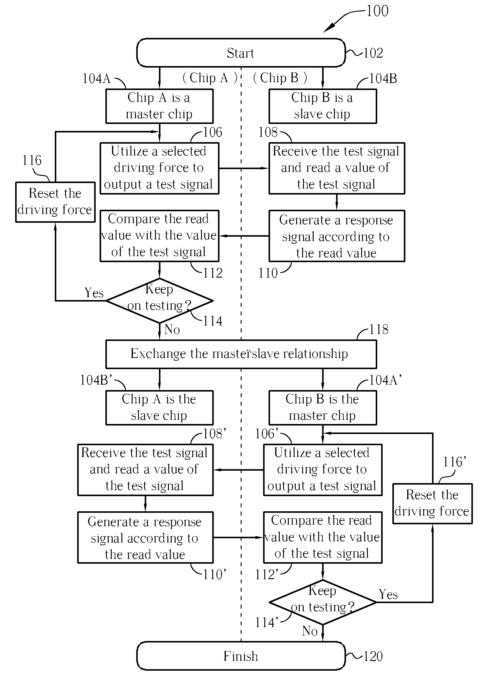
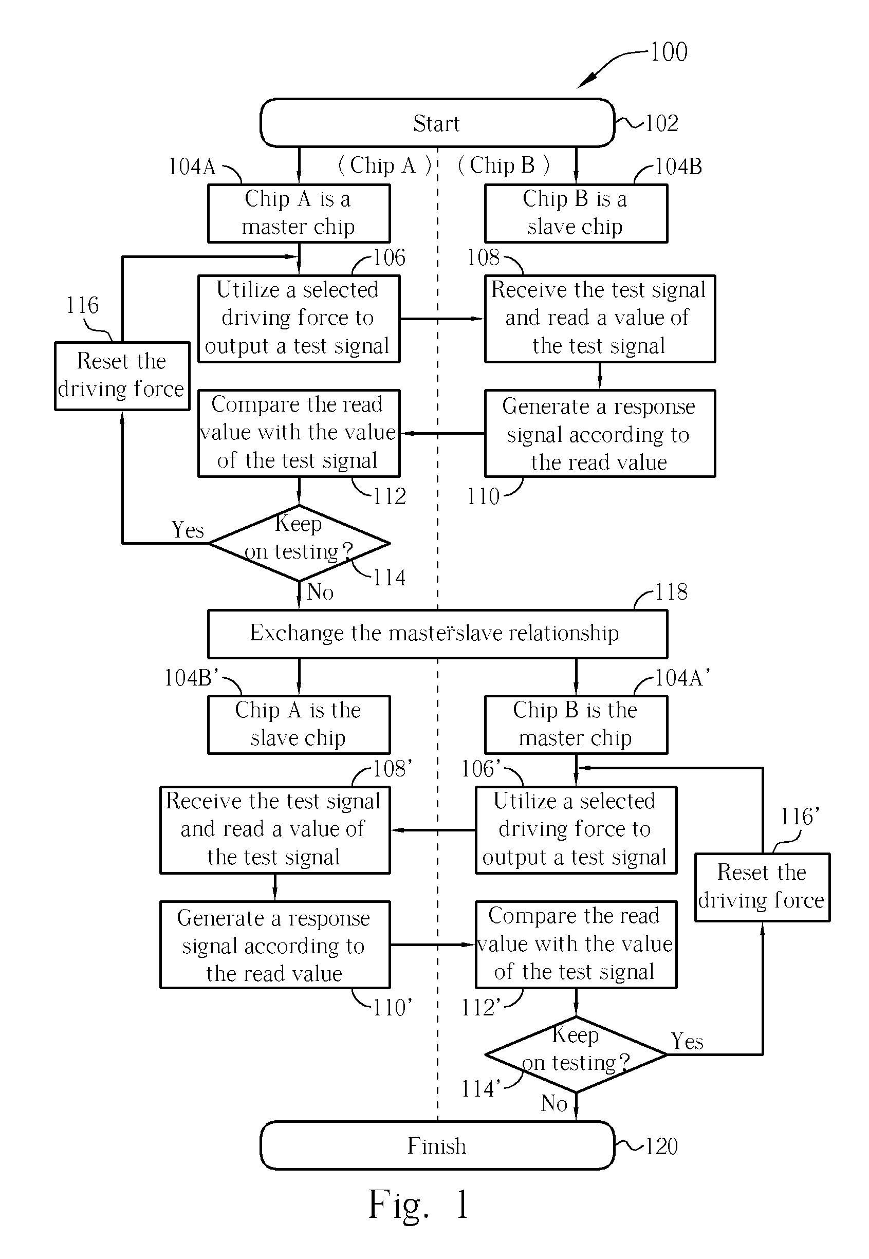
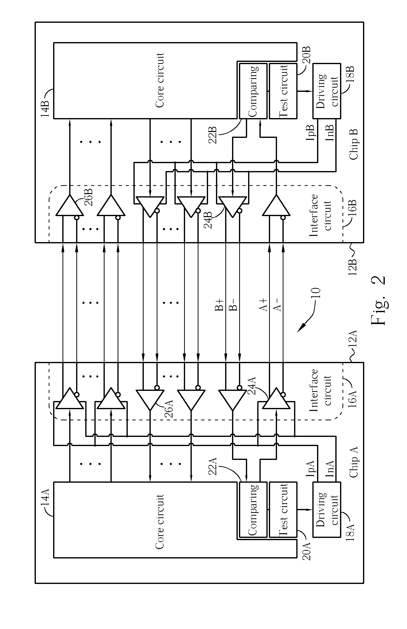
[0022]Please refer to FIG. 1, which is a flowchart 100 of the calibration technique of an embodiment according to the present invention. In an electronic system, two connected chips A and B can detect acceptable signal driving forces through using the flowchart 100 in order to ensure that signals generated from each chip can be correctly read by another chip. The flowchart 100 is illustrated as follows:

[0023]Step 102: Start. The flowchart 100 can start when the chip has sufficient power supply. For example, if the flowchart 100 is implemented in a computer system, when the computer system is supplied with an external power, the flowchart 100 can start. After completely performing the flowchart 100, each chip can correctly exchange data, and the BIOS of the computer system can be loaded such that the booting procedure can be continuously performed.

[0024]Step 104A-step 104B: When the flowchart 100 is performed on two chips A and B connected to each other, chip A can first be the maste...


PUM


Abstract

A calibrating method for adjusting related parameters when a first chip and a second chip switch signals is disclosed. The calibrating method includes: utilizing the first chip to output a test signal through using a first driving force in order to represent a test value; utilizing the second chip to receive the test signal and utilizing the second chip to read the test signal to determine a value; and performing a comparison step for comparing the value with the test value to detect whether said value complies with the test value.

Description

BACKGROUND OF THE INVENTION[0001]1. Field of the Invention[0002]The invention relates to a calibrating method for adjusting signal driving parameters between chips and a related apparatus thereof, and more particularly, to a calibrating method for performing signal tests between chips to test a better driving force and a related apparatus thereof.[0003]2. Description of the Prior Art[0004]Electronic systems such as microprocessor systems have become highly important hardware foundations in our modern information society. A complicated electronic system utilizes many chips having different functions that co-operate with each other to achieve the complete function of the system. For example, a personal computer system comprises a CPU, chipsets (e.g. the south bridge / north bridge chipset or a chipset integrating the south bridge and north bridge), and a memory module. The chips are utilized to control data exchange between a peripheral device and the chipset. For example, a hard disk d...

Claims


Application Information

Patent Timeline
Patent Type & Authority Patents(United States)
IPC IPC(8): G01R31/30G06F11/00
CPCG06F13/4269
Inventor KUO, HUNG-YICHEN, JENNY
Owner VIA TECH INC
Why Eureka
Try Eureka