Thermal tunneling gap diode with integrated spacers and vacuum seal

a gap diode and gap diode technology, applied in the field of cooling devices, can solve problems such as difficult manufacturing, and achieve the effects of reducing or eliminating the problem of thermal conduction between layers, reducing costs, and reducing the cost of creating gap diode devices

Inactive Publication Date: 2009-09-15
BOREALIS TECH LTD
View PDF114 Cites 9 Cited by
  • Summary
  • Abstract
  • Description
  • Claims
  • Application Information

AI Technical Summary

Benefits of technology

[0015]The approaches disclosed above utilize widely-applied silicon on insulator wafer bonding techniques to bond two silicon wafers with thin oxide layers in between. By not bonding the entire surface, for instance by trapping a small particle between two silicon wafers, due to the mechanical properties of silicon, a non-bonded area (void) of 5000 times the size (height) of the particle is created. Consequently, if two particles are spaced less than 2×5000 times the size of the particles, an even larger void is created. Using this idea, it is possible to form small “spacers” that keep the wafers at the desired distance of 5-10 nm without causing electrical or thermal “shorts”.
[0016]This invention provides the simplicity of a layered structure to provide electrode separation without the use of active elements, and therefore problems of thermal conduction between the layers is reduced or eliminated.
[0017]Furthermore, this method of creating gap diode devices is inexpensive as it does not require active elements such as piezoelectric actuators to build and maintain the gap.
[0018]Furthermore, this invention discloses methods for manufacturing thermotunneling converters on a large scale, thus reducing costs and increasing the scope of potential applications.

Problems solved by technology

One drawback is that the device must contain some 106 elements in order to provide reasonable efficiency, and this is difficult to manufacture.
A further drawback results from the losses due to thermal conduction: although the oxide spacers have a small contact coefficient with the emitter and collector elements, which minimizes thermal conduction, the number of elements required for the operation of the device means that thermal conduction is not insignificant.

Method used


Image

  • Thermal tunneling gap diode with integrated spacers and vacuum seal
  • Thermal tunneling gap diode with integrated spacers and vacuum seal
  • Thermal tunneling gap diode with integrated spacers and vacuum seal

Examples


example

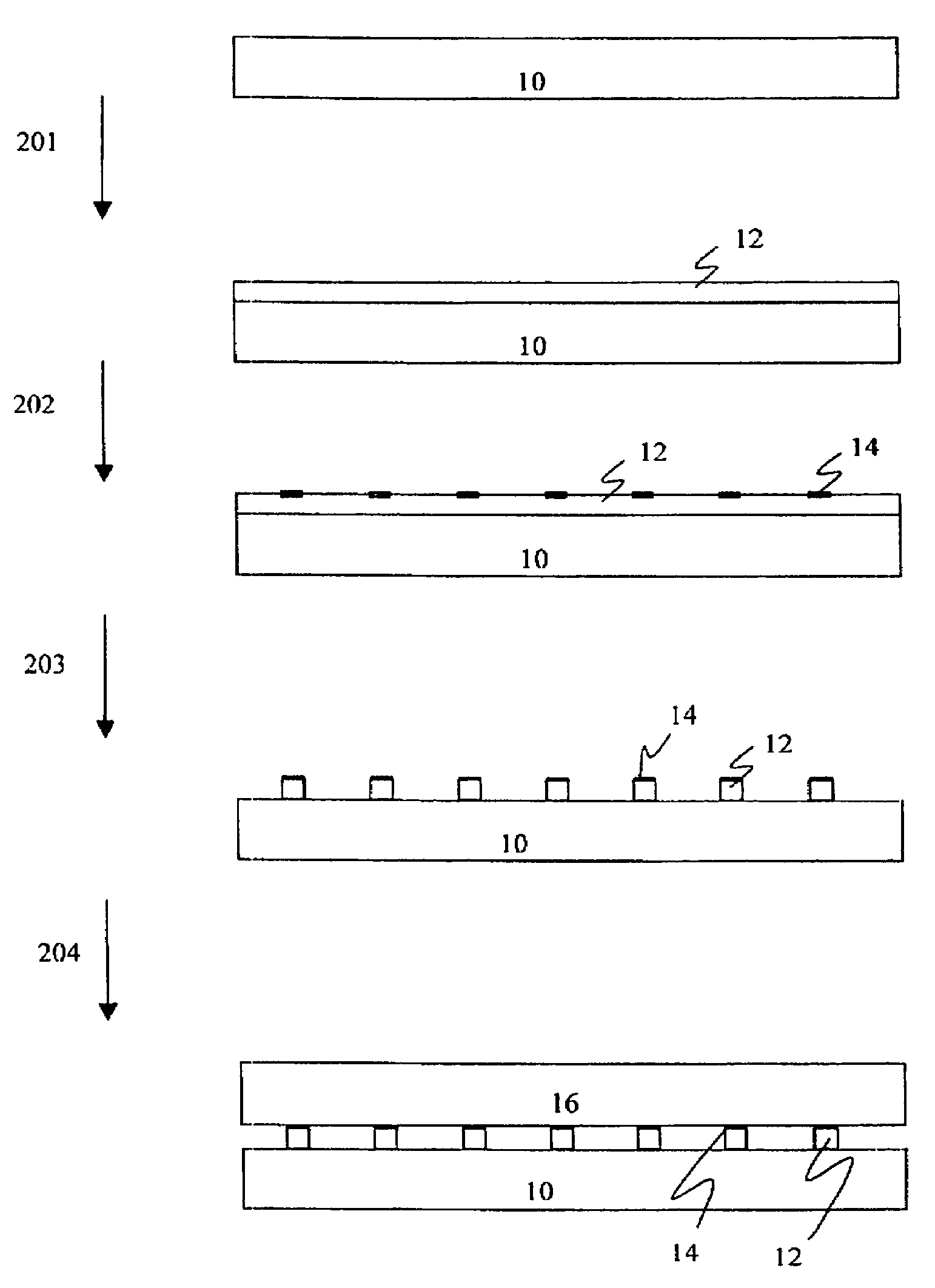
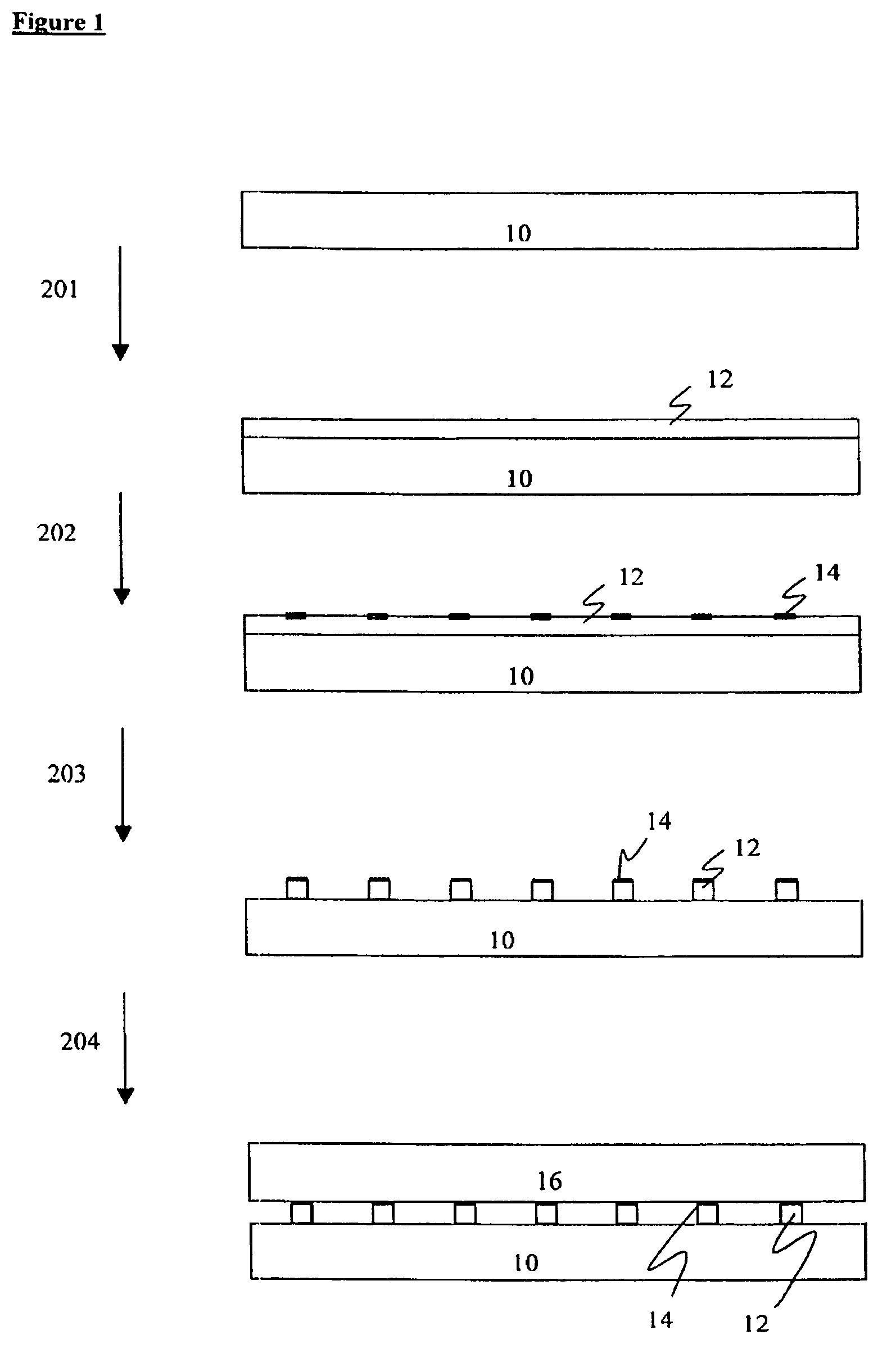
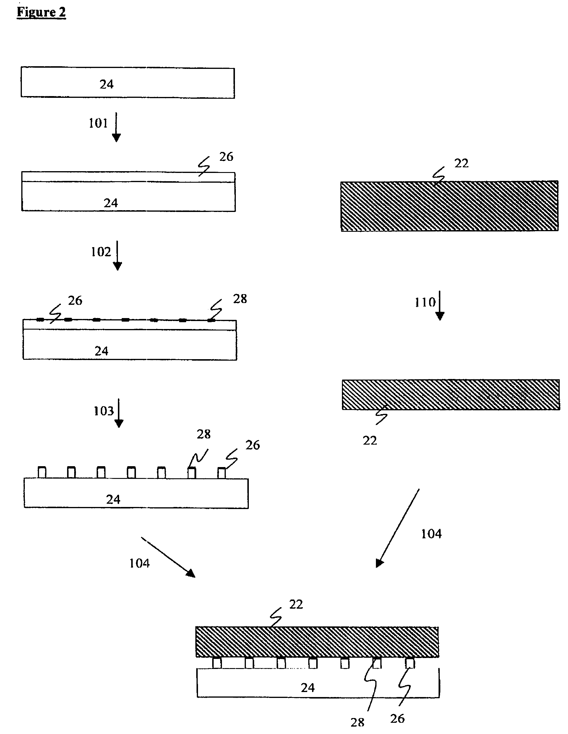
[0048]Referring now to FIG. 4, shown is a circular silicon wafer 40 of 200 mm diameter. Arranged on the surface of wafer 40 are a plurality of rectangular electrodes 42, 25×20 mm2 in size. Rectangular electrodes 42 fill as much surface space of wafer 40 as is possible, while leaving an aisle 43 of 2 mm between each device. Referring now to FIG. 5, wafer 40 is oxidized to create an oxide layer 41 on the entire surface of wafer 40. FIG. 6 shows wafer 40 after dots have been formed on rectangles 42 and the oxide in between the dots removed. Oxide is also removed from aisles 43 in between rectangles 42.

[0049]It is understood that a second wafer of identical dimensions to wafer 40 is attached to wafer 40 in order to create a sheet of thermotunneling converters, which can then be cut into individual converters.

[0050]FIG. 7 shows one rectangular electrode 42 of wafer 40. Rectangular electrode 42 comprises a silicon wafer covered with a layer of oxidized silicon. A bond pad 46 of 5×20 mm is...


PUM


Abstract

A thermionic or thermotunneling gap diode device consisting of two silicon electrodes maintained at a desired distance from one another by means of spacers. These spacers are formed by oxidizing one electrode, protecting certain oxidized areas and removing the remainder of the oxidized layer. The protected oxidized areas remain as spacers. These spacers have the effect of maintaining the electrodes at a desired distance without the need for active elements, thus greatly reducing costs.

Description

CROSS-REFERENCE TO RELATED APPLICATIONS[0001]This application claims the benefit of U.S. Provisional App. No. 60 / 662,058, filed Mar. 14, 2005.BACKGROUND OF THE INVENTION[0002]This present invention is directed towards devices for cooling. In particular it is directed toward devices for cooling Integrated Circuits, such as high-performance Micro-Processors, VLSI chipsets, Infra-Red imaging sensors, and the like.[0003]In U.S. Pat. No. 6,720,704 diode devices are disclosed in which the separation of the electrodes is set and controlled using piezo-electric, electrostrictive or magnetostrictive actuators. This avoids problems associated with electrode spacing changing or distorting as a result of heat stress. In addition it allows the operation of these devices at electrode separations which permit quantum electron tunneling between them. Pairs of electrodes whose surfaces replicate each other are also disclosed. These may be used in constructing devices with very close electrode spacin...

Claims


Application Information

Patent Timeline
Patent Type & Authority Patents(United States)
IPC IPC(8): H01L29/40
CPCH01J45/00H01L23/34H01L2924/0002H01L2924/00
Inventor WALITZKI, HANS JUERGEN
Owner BOREALIS TECH LTD
Why Eureka
Try Eureka