Stackable semiconductor package
a stackable semiconductor and package technology, applied in semiconductor devices, semiconductor/solid-state device details, electrical devices, etc., can solve the problems of affecting the overhang portion may shake or sway, and the overall thickness of the conventional stackable semiconductor package b>1/b> cannot be effectively reduced, so as to reduce the overall thickness of the stackable semiconductor package and reduce the thickness of the second substra
- Summary
- Abstract
- Description
- Claims
- Application Information
AI Technical Summary
Benefits of technology
Problems solved by technology
Method used
Image

Examples
first embodiment
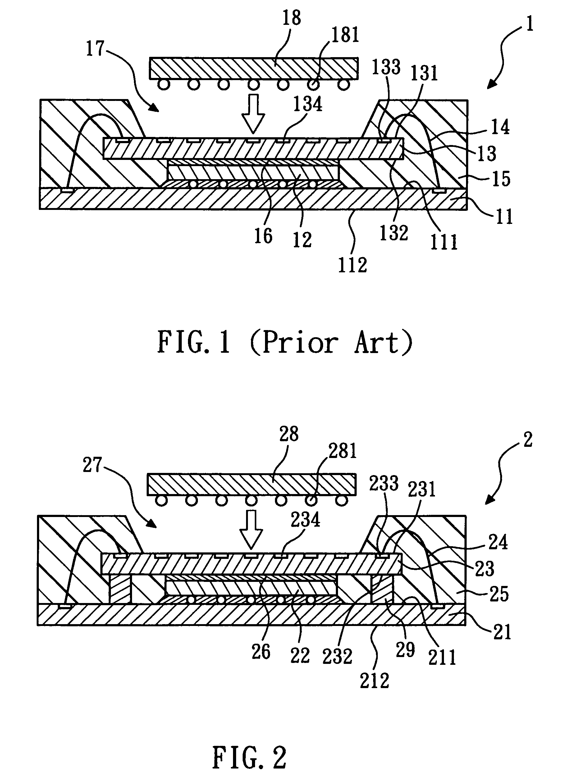
[0015]FIG. 2 is a schematic sectional view of the stackable semiconductor package according to the present invention. The stackable semiconductor package 2 comprises a first substrate 21, a semiconductor device 22, a second substrate 23, a plurality of first wires 24, a supporting element 29, and a first molding compound 25. The first substrate 21 has a first surface 211 and a second surface 212. The semiconductor device 22 is disposed on the first surface 211 of the first substrate 21, and is electrically connected thereto. In the present embodiment, the semiconductor device 22 is a chip, which is attached to the first surface 211 of the first substrate 21 by means of a flip chip.
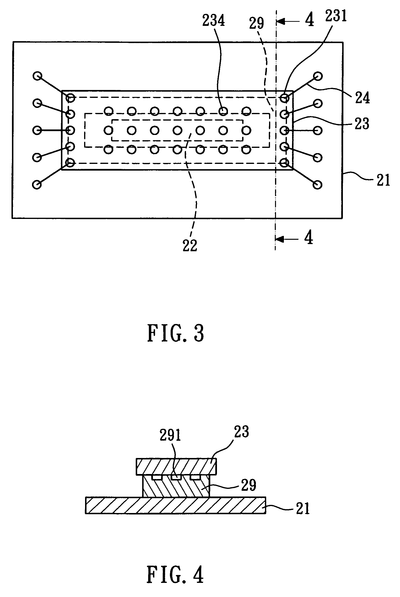
[0016]The second substrate 23 is adhered to the semiconductor device 22 by the use of an adhesive layer 26, and has a first surface 231 and a second surface 232, wherein the first surface 231 has a plurality of first pads 233 and a plurality of second pads 234 disposed thereon. From a top view, the area of...
second embodiment
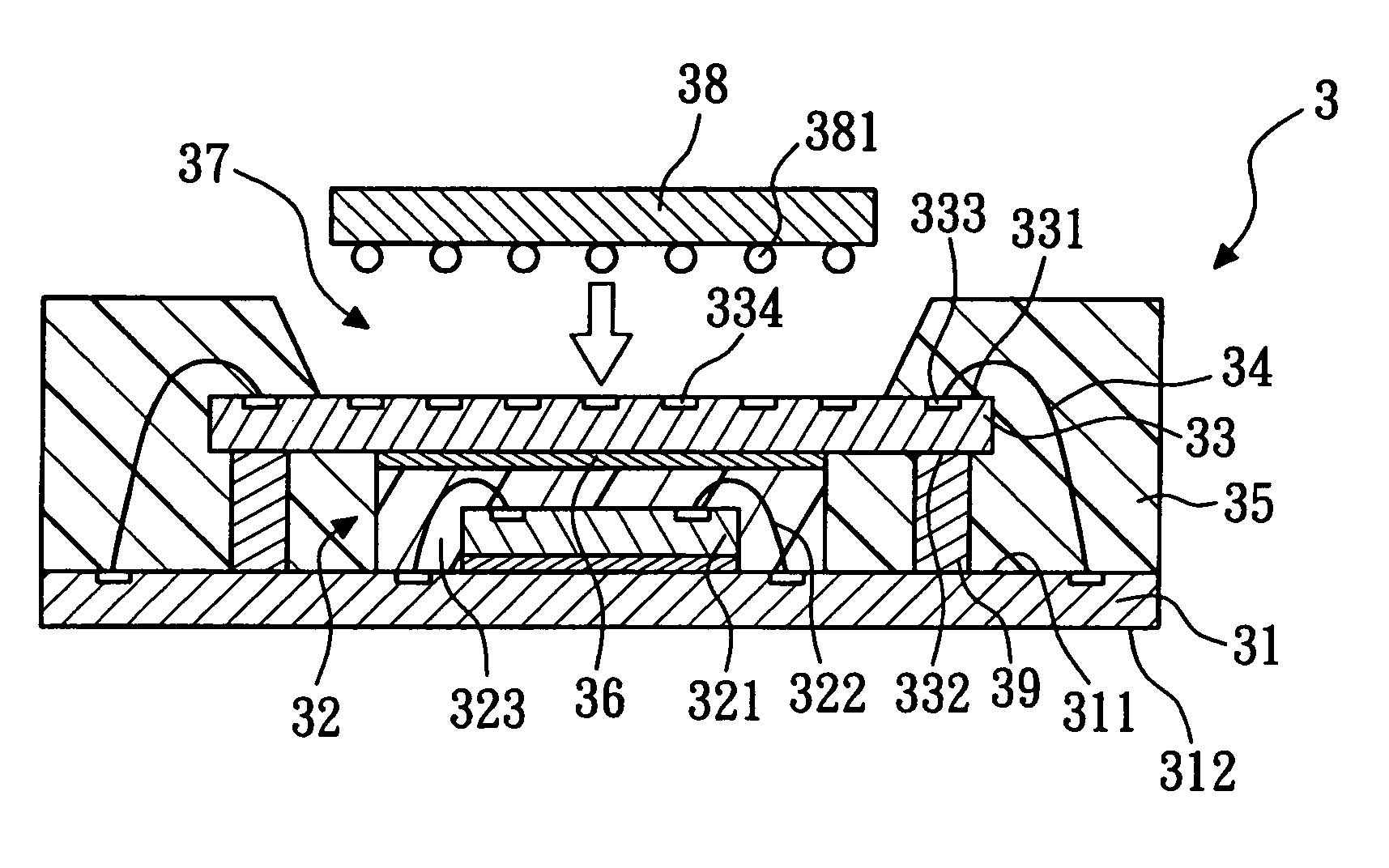
[0021]FIG. 5 is a schematic sectional view of the stackable semiconductor package according to the present invention. The stackable semiconductor package 3 comprises a first substrate 31, a semiconductor device 32, a second substrate 33, a plurality of first wires 34, a supporting element 39, and a first molding compound 35. The first substrate 31 has a first surface 311 and a second surface 312. The semiconductor device 32 is disposed on the first surface 311 of the first substrate 31, and is electrically connected thereto. In the present embodiment, the semiconductor device 32 is a sub-package including a chip 321, a plurality of second wires 322, and a second molding compound 323. The chip 321 is adhered to the first surface 311 of the first substrate 31. The second wires 322 electrically connect the chip 321 to the first surface 311 of the first substrate 31. The second molding compound 323 encapsulates the chip 321, the second wires 322, and a portion of the first surface 311 o...
PUM
 Abstract
Description
Claims
Application Information
 - R&D Engineer
- R&D Manager
- IP Professional
- Industry Leading Data Capabilities
- Powerful AI technology
- Patent DNA Extraction
Browse by: Latest US Patents, China's latest patents, Technical Efficacy Thesaurus, Application Domain, Technology Topic.
© 2024 PatSnap. All rights reserved.Legal|Privacy policy|Modern Slavery Act Transparency Statement|Sitemap