Supercharge Your Innovation With Domain-Expert AI Agents!

Data conversion circuit, and semiconductor memory apparatus using the same

semiconductor technology, applied in the field of semiconductor memory apparatus, can solve problems such as the decrease in the integration of the semiconductor memory apparatus, and achieve the effect of reducing the area where a data conversion circuit is disposed

Active Publication Date: 2009-09-29
SK HYNIX INC
View PDF27 Cites 0 Cited by
  • Summary
  • Abstract
  • Description
  • Claims
  • Application Information

AI Technical Summary

Benefits of technology

[0011]An embodiment of the present invention provides a data conversion circuit that can convert serial data to parallel data and convert parallel data to serial data using a single data conversion circuit.
[0012]Another embodiment of the present invention provides a semiconductor memory apparatus that can reduce an area where a data conversion circuit is disposed.
[0013]Still another embodiment of the present invention provides a data conversion method that can convert serial data to parallel data and convert parallel data to serial data using a single data conversion circuit.

Problems solved by technology

This results in a decrease in integration of the semiconductor memory apparatus.

Method used


Image

  • Data conversion circuit, and semiconductor memory apparatus using the same
  • Data conversion circuit, and semiconductor memory apparatus using the same
  • Data conversion circuit, and semiconductor memory apparatus using the same

Examples


Embodiment Construction

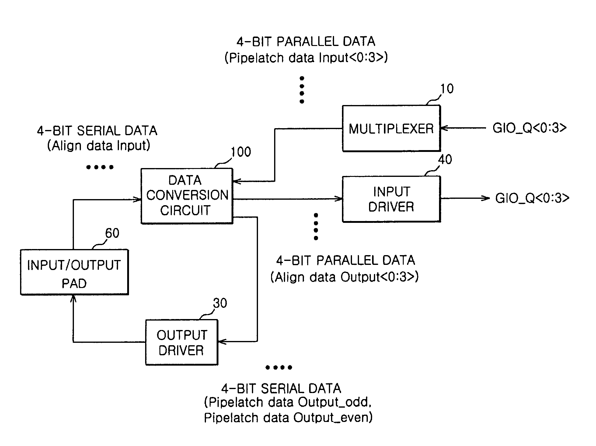
[0020]Hereinafter, an exemplary embodiment of a data conversion circuit of a semiconductor memory apparatus according to the present invention will be described in detail with reference to the accompanying drawings.

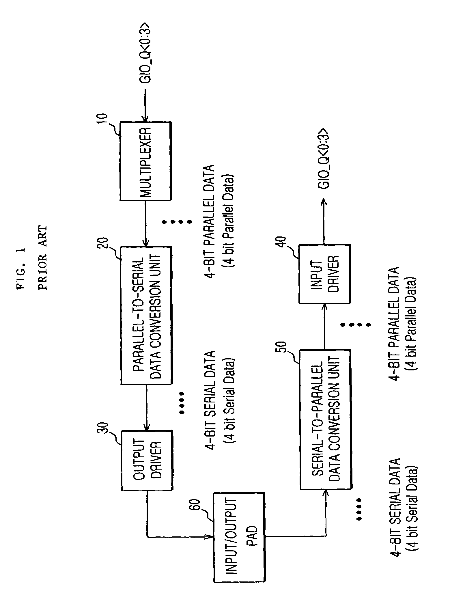
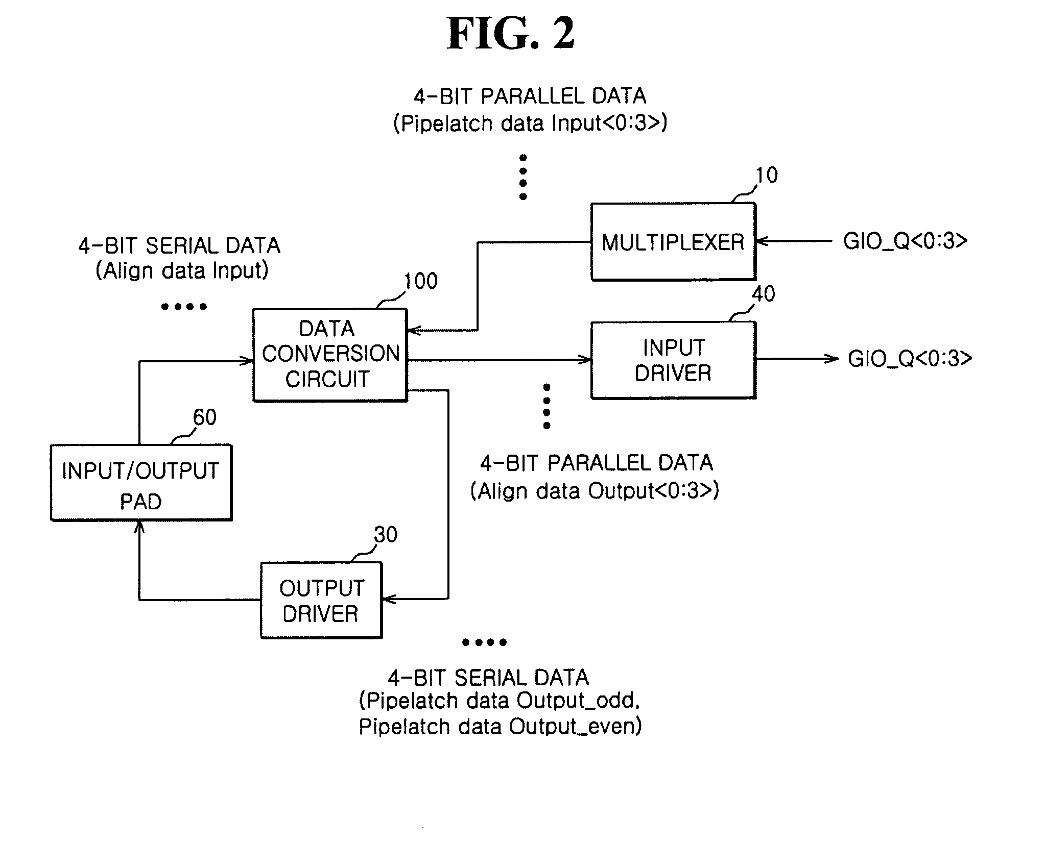
[0021]Referring to FIG. 2, a semiconductor memory apparatus, to which a data conversion circuit 100 according to an embodiment of the present invention is applied, includes a multiplexer 10, an output driver 30, an input / output pad 60, and an input driver 40.

[0022]When a read command is input, the multiplexer 10 transmits 4-bit parallel data Pipelatch data Input0:3>, which is transmitted from the input / output lines GIO_Q0:3>, to the data conversion circuit 100. At this time, the data conversion circuit 100 converts the 4-bit parallel data Pipelatch data Input0:3> to 4-bit serial data Pipelatch data Output_odd and Pipelatch data Output_even. Subsequently, the converted 4-bit serial data Pipelatch data Output_odd and Pipelatch data Output_even are transmitted to the input / o...


PUM


Abstract

A data conversion circuit for a semiconductor memory apparatus includes a data conversion unit that has a plurality of latches for storing input data and outputting stored data as output data in response to a clock, and an operation mode selection unit that selects either a first operation mode to convert serial data to parallel data during a write operation or a second operation mode to convert parallel data to serial data during a read operation, to thereby drive the data conversion unit.

Description

CROSS-REFERENCE TO RELATED PATENT APPLICATION[0001]This application claims the benefit of Korean Patent Application No. 10-2006-0112619, filed on Nov. 15, 2006, in the Korean Intellectual Property Office, the disclosure of which is incorporated herein in its entirety by reference.BACKGROUND OF THE INVENTION[0002]1. Technical Field[0003]The present invention relates to a semiconductor memory apparatus, and in particular, to a data conversion circuit of a semiconductor memory apparatus, a semiconductor memory apparatus using the same, and a data conversions method.[0004]2. Related Art[0005]Generally, a semiconductor memory apparatus receives serial data through a single input path. The semiconductor memory apparatus internally converts serial data to parallel data and stores the converted parallel data in memory cells. When the stored data is output, parallel data is converted to serial data. Accordingly, in order to input data to and store data in the semiconductor memory apparatus, ...

Claims


Application Information

Patent Timeline
Patent Type & Authority Patents(United States)
IPC IPC(8): G11C7/00
CPCG11C7/1006G11C7/1072G11C11/4096G11C7/1066G11C7/1045G11C2207/107G11C7/10G11C7/22
Inventor KIM, JAE-HEUNG
Owner SK HYNIX INC
Features
  • R&D
  • Intellectual Property
  • Life Sciences
  • Materials
  • Tech Scout
  • Unparalleled Data Quality
  • Higher Quality Content
  • 60% Fewer Hallucinations
Learn More