

Semiconductor device and method of manufacturing semiconductor device
a semiconductor device and semiconductor technology, applied in the direction of sustainable manufacturing/processing, final product manufacturing, printed circuit aspects, etc., can solve the problems of oxidized solder provided on the package board (land), disadvantageous oxidation of bare copper, and difficulty in wetting the solder on the end surface,
- Summary
- Abstract
- Description
- Claims
- Application Information
AI Technical Summary
Benefits of technology
Problems solved by technology
Method used
Image

Examples
Embodiment Construction
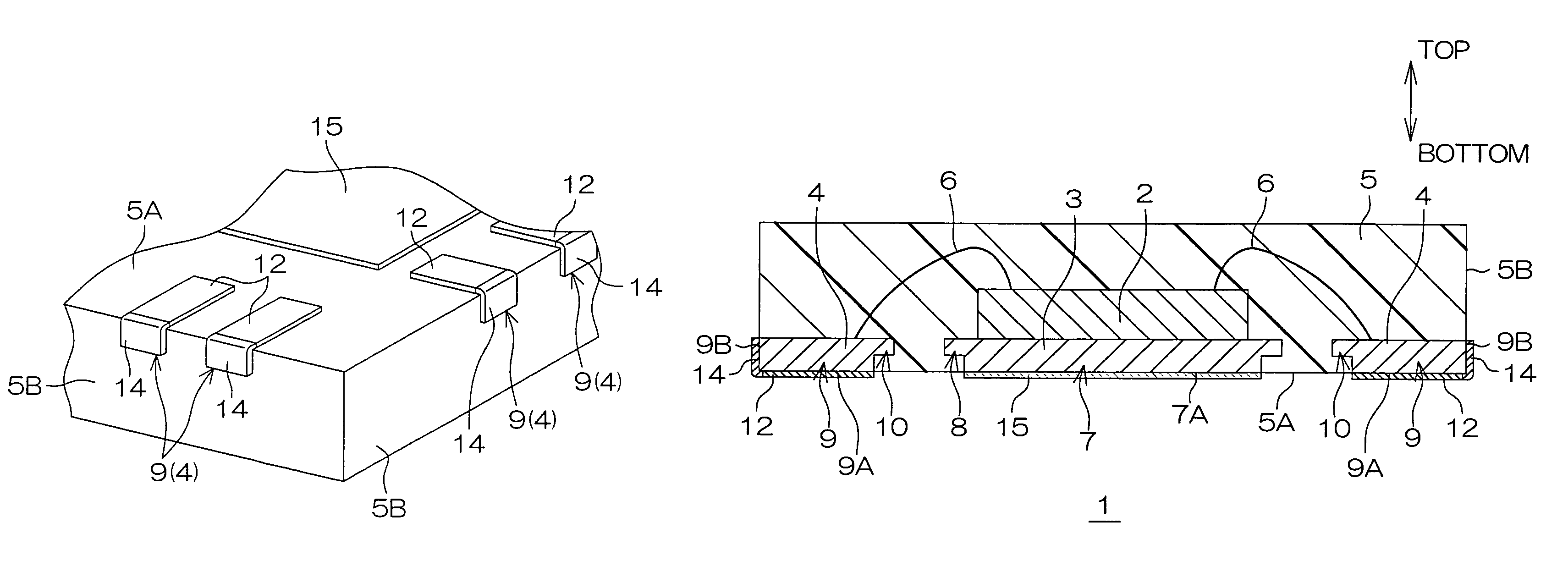
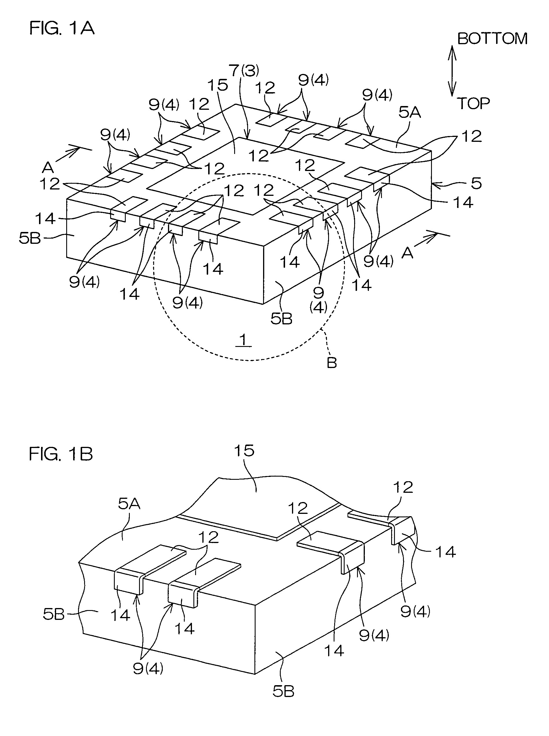
[0034]FIG. 1A is a schematic perspective view of a semiconductor device 1 according to an embodiment of the present invention as viewed obliquely from above. FIG. 1B is an enlarged view of a part of the semiconductor device 1 surrounded by a broken circle B in FIG. 1A. FIG. 2 is a schematic sectional view of the semiconductor device 1 taken along the line A-A in FIG. 1A.
[0035]A QFN is applied to the semiconductor device 1. This semiconductor device 1 includes a semiconductor chip 2, a die pad 3 supporting the semiconductor chip 2, a plurality of leads 4 electrically connected with the semiconductor chip 2 and sealing resin 5 sealing these elements.
[0036]The semiconductor chip 2 is die-bonded onto the die pad 3 while directing the surface (device forming surface) provided with functional elements upward. A plurality of pads (not shown) are formed on the surface of the semiconductor chip 2 by partially exposing a wiring layer from a surface protective film. The respective pads are ele...
PUM
 Abstract
Description
Claims
Application Information