Wafer sawing method

a cutting method and cutting tool technology, applied in the field of semiconductor manufacturing technology, can solve the problems of chip malfunction, accumulated errors caused by tilt angle or cutting tool moving distance, and inability to meet the needs of manufacturing, etc., to achieve the effect of precise and rapid cutting process and superior manufacturing yield

Inactive Publication Date: 2009-11-03
ADVANCED SEMICON ENG INC
View PDF1 Cites 0 Cited by
  • Summary
  • Abstract
  • Description
  • Claims
  • Application Information

AI Technical Summary

Benefits of technology

[0009]The present invention is directed to a wafer sawing method in which a precise and rapid cutting process can be performed, and superior manufacturing yield can be achieved.
[0015]In the present invention, the cutting tool and the carrier are precisely positioned according to the strip-shaped adhesives or the fiducial mark on the carrier, such that the devices or the circuits on the chips can be prevented from being damaged due to the errors occurring in the sawing process. Moreover, the adverse impact on the hermetic space between the carrier and each of the chips can be avoided as well, so as to ensure the protection for the devices on the chips during the wafer sawing process or the subsequent processes.

Problems solved by technology

However, errors arisen from tilt angles or a moving distance of the cutting tool may occur when the cutting tool is moved, and each of the longitudinal sawing lines and each of the latitudinal sawing lines use the previous longitudinal sawing line and the previous latitudinal sawing line as the standard.
As such, during the implementation of the wafer sawing process, accumulated errors caused by the tilt angles or the moving distance of the cutting tool are apt to take place after the longitudinal sawing lines and the latitudinal sawing lines are formed, i.e., after the cutting tool longitudinally or latitudinally shifts by an excessive distance.
Consequently, when the cutting tool performs the sawing operation on the wafer, it is very much likely to damage the devices or circuits on the chips, resulting in malfunctions of the chips.
On the other hand, the errors occurring in the wafer sawing process may affect the hermetic space between the carrier and each of the chips, resulting in failure to protect the devices on the surfaces of the chips.
The devices on the chips may accordingly be contaminated by coolant for the sawing operation or by particles of materials in subsequent processes, reducing process yield of the wafer.

Method used


Image

  • Wafer sawing method
  • Wafer sawing method
  • Wafer sawing method

Examples


Embodiment Construction

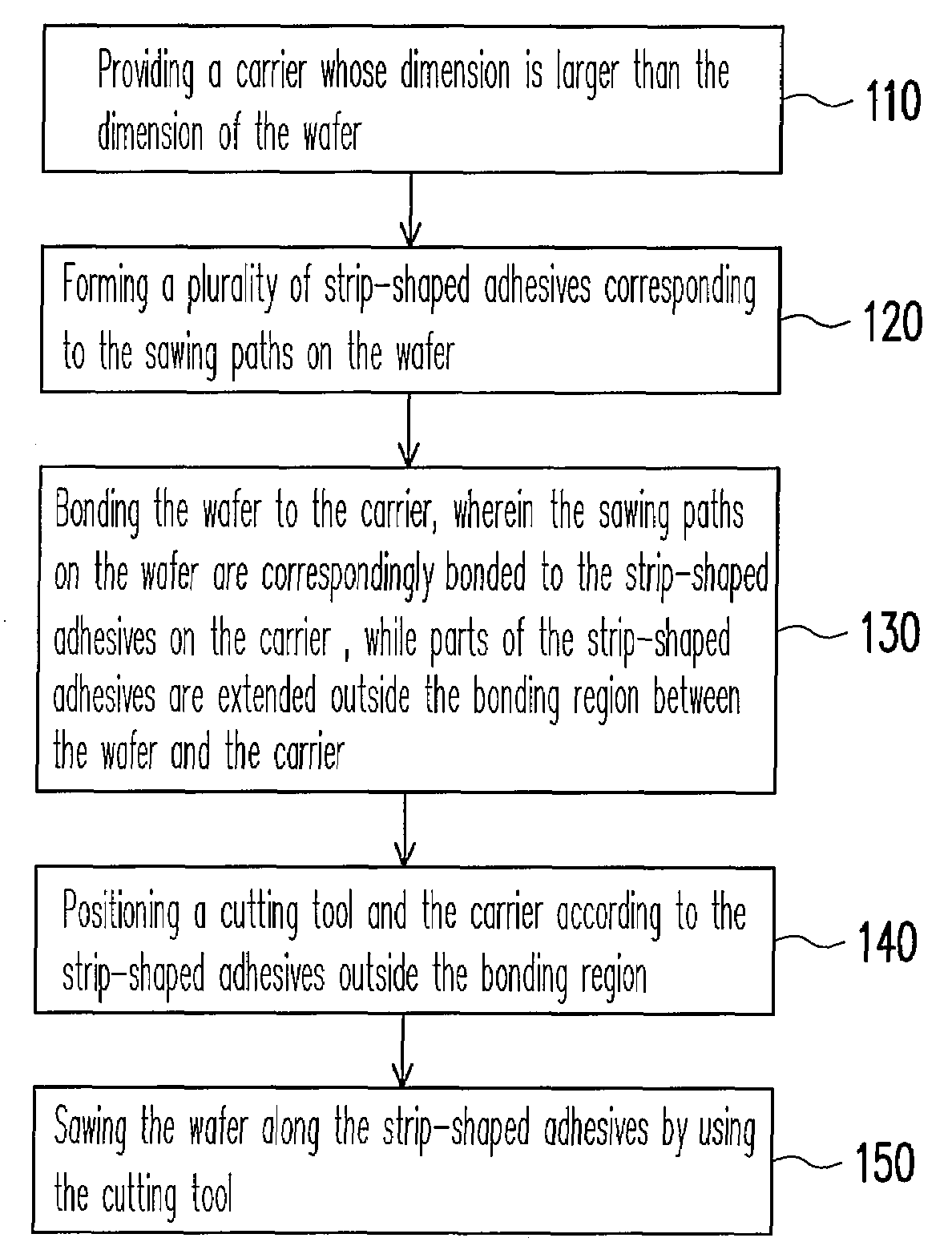
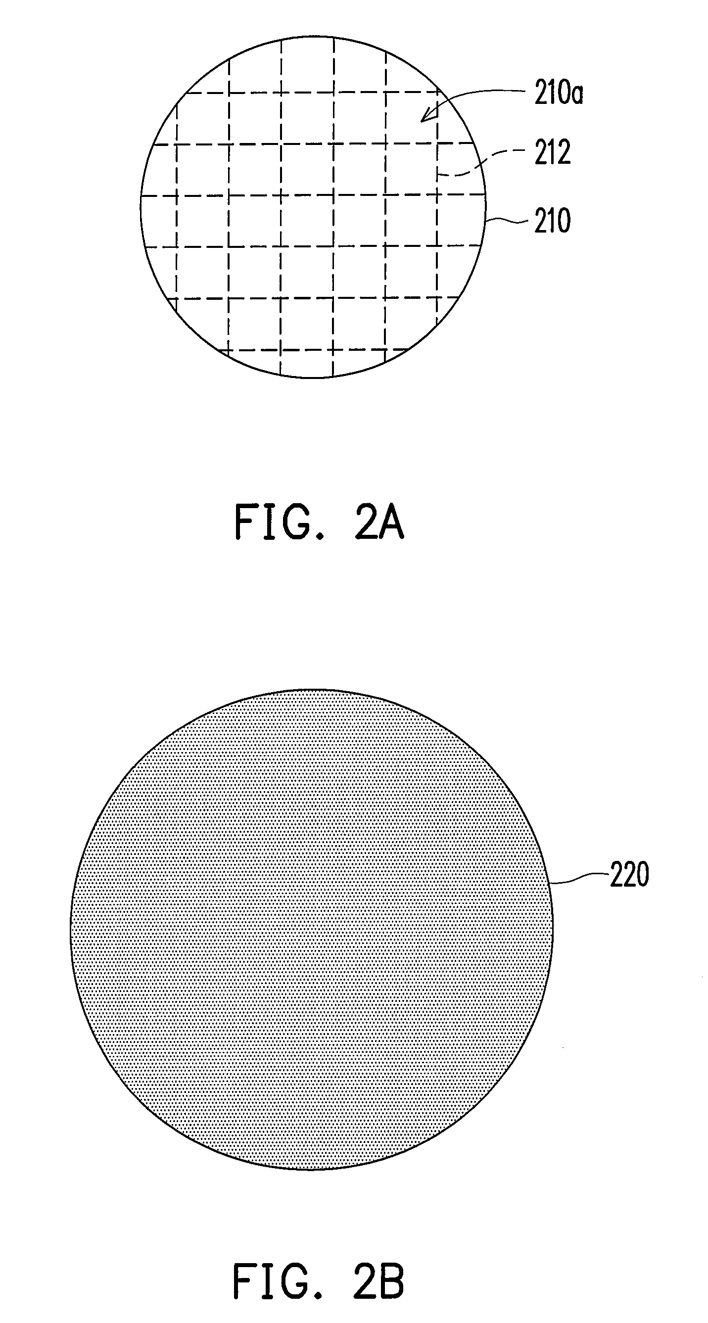
[0026]In the present invention, strip-shaped adhesives or a fiducial mark is formed on a carrier for positioning a cutting tool and the carrier. A method of forming the strip-shaped adhesives includes applying an adhesive bonding technique through which a plurality of the strip-shaped adhesives corresponding to sawing paths of a wafer is formed by coating the adhesives on the carrier. Besides, during the adhesive coating process, the strip-shaped adhesives are extended outside a bonding region between the wafer and the carrier, such that parts of the strip-shaped adhesives are exposed outside the wafer after the wafer and the carrier are bonded together. The exposed parts of the strip-shaped adhesives can be used for positioning the cutting tool and the carrier. In addition, the fiducial mark can be formed individually or together with the strip-shaped adhesives on the carrier, so as to position the cutting tool and the carrier. The fiducial mark is formed during the fabrication of ...


PUM


Abstract

A wafer sawing method for sawing a wafer by using a cutting tool is provided. Sawing paths are formed on a surface of the wafer. In the wafer sawing method, a carrier on which strip-shaped adhesives or at least a fiducial mark is formed is firstly provided. The dimension of the carrier is greater than the dimension of the wafer. Next, the surface of the wafer is bonded to the carrier, and the strip-shaped adhesives or the fiducial mark is extended or located outside a bonding region between the wafer and the carrier. Here, the surface of the wafer faces the carrier. The cutting tool and the carrier are positioned according to the strip-shaped adhesives or the fiducial mark outside the bonding region. The wafer is then sawed by using the cutting tool. The wafer sawing method provides a precise and rapid sawing process and achieves superior productive yield.

Description

CROSS-REFERENCE TO RELATED APPLICATION[0001]This application claims the priority benefit of Taiwan application serial no. 96113436, filed on Apr. 17, 2007. The entirety the above-mentioned patent application is hereby incorporated by reference herein and made a part of specification.BACKGROUND OF THE INVENTION[0002]1. Field of the Invention[0003]The present invention relates to a semiconductor manufacturing technology, and more particularly, to a wafer sawing method.[0004]2. Description of Related Art[0005]With recent advancement of semiconductors and packaging technologies, the fabrication of micro devices including micro-electromechanical devices or electro-optical devices is currently achieved by adopting a prevailing wafer packaging technique rather than a chip packaging technique. Thereby, packaging costs are reduced, and the requirements for lightweight, slimness, compactness, and small volume are satisfied. Generally, after devices on a wafer are completely manufactured in th...

Claims


Application Information

Patent Timeline
Patent Type & Authority Patents(United States)
IPC IPC(8): H01L21/00
CPCB28D5/0082H01L21/67282H01L21/67092
Inventor PENG, SHENG-YANG
Owner ADVANCED SEMICON ENG INC
Why Eureka
Try Eureka