Fabricating substrates having low inductance via arrangements

a technology of fabricating substrates and via arrangements, which is applied in the direction of auxillary welding devices, instruments, soldering apparatus, etc., can solve the problems of proportion of the integrated circuit negatively affecting other portions of the integrated circuit, and achieve the effect of increasing the capacitance and minimizing the inductan

Inactive Publication Date: 2009-11-10
GLOBALFOUNDRIES INC
View PDF4 Cites 2 Cited by
  • Summary
  • Abstract
  • Description
  • Claims
  • Application Information

AI Technical Summary

Benefits of technology

[0009]In view of the above, it would be beneficial to have a multilayer ceramic (MLC) substrate in which the configuration of the vias minimizes the inductance introduced by the via-field and thereby, as a secondary affect, increases the capacitive effect. Moreover, it would be beneficial to have an integrated circuit device that utilizes such a via configuration. The illustrative embodiments provide such a multilayer ceramic substrate and integrated circuit device.
[0010]The illustrative embodiments take advantage of two primary characteristics of inductance. First, parallel paths, i.e., inductors that are in parallel, divide. That is, if there are two parallel inductors having an inductance of 1, the resulting combined inductance is 0.5. The second characteristic is that the inductance decreases in relative proportion to the log of the distance between the current paths. Thus, using these two characteristics, by introducing additional parallel current paths in the via arrangement of a MLC substrate, the inductance of the via field may be reduced and the capacitive effect may be increased.
[0011]Thus, with the MLC substrate and via arrangement of the illustrative embodiments, the via-field inductance for a given contact pad array is reduced by the introduction of T-jogs and additional vias in the MLC substrate. These T-jogs and additional vias form additional current paths that cause additional parallel inductances that reduce the via-field inductance. In addition, these T-jogs reduce the area between current paths and thereby, further reduce the inductance of the via field.
[0012]In one illustrative embodiment, the additional T-jogs and vias are added to a center or inner portion of a contact pad array. The T-jogs are comprised of two jogs in a wiring layer of the MLC, each jog being toward a via associated with an adjacent contact pad in the contact pad array. These additional T-jogs and vias form additional current paths parallel to the existing ones which thus, reduce the total inductance of the via-field.
[0016]The plurality of vias may comprise at least three vias. The T-jog configuration may be associated with an inner via of the at least three vias. The T-jog may introduce at least one additional current path in a via field of the substrate that reduces an inductance of the via field.

Problems solved by technology

The use of such decoupling networks is important in the formation of integrated circuit devices which, because of their compact and ever decreasing size, are prone to having one portion of the integrated circuit negatively affecting other portions of the integrated circuit.
Thus, straight vias situated at relatively large surface pad spacing distances represent the least beneficial arrangement of vias with regard to reducing the inductance of the capacitor since the distance between vias is maximized in such an arrangement.

Method used


Image

  • Fabricating substrates having low inductance via arrangements
  • Fabricating substrates having low inductance via arrangements
  • Fabricating substrates having low inductance via arrangements

Examples


Embodiment Construction

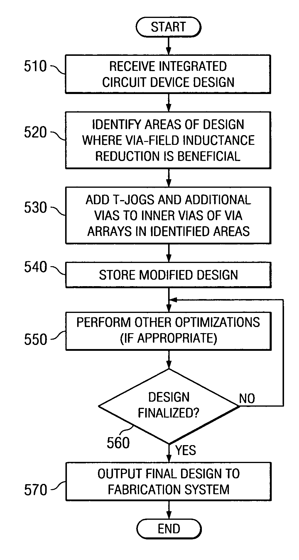
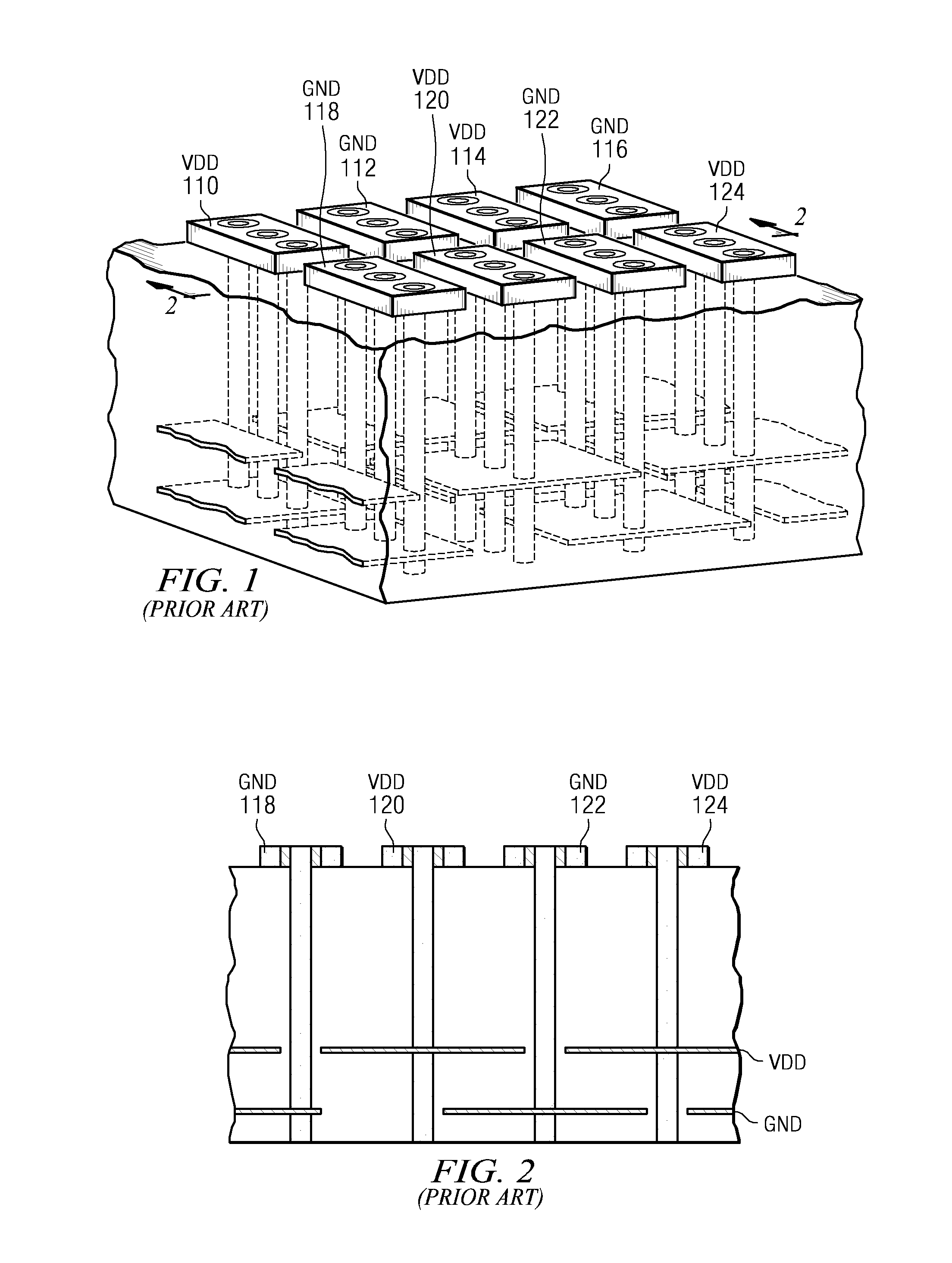
[0028]As previously described above, conventionally, vias are formed in a multilayer ceramic (MLC) substrate as straight via connections between a surface pad connection and an internal plane, e.g., the internal voltage (VDD) or ground (GND) planes. Such an arrangement does not minimize the inductance generated by the vias, i.e., the via-field inductance, since the distance between the vias tends to be maximized in such an arrangement.

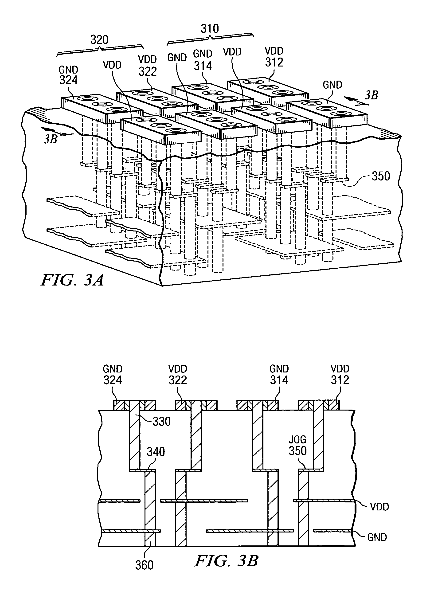
[0029]One solution to reduce the inductance generated by the via-field is to introduce single “jogs” in the vias so as to bring them closer together, i.e. reduce the distance between the vias. These single “jogs” are essentially portions of the vias that run perpendicular to the conventional via, i.e. parallel to the internal planes of the MLC. The “jogs” may be formed as horizontal wirings in a wiring plane of the MLC.

[0030]FIGS. 3A and 3B are exemplary diagrams illustrating the arrangement of the vias in accordance with a known alternative configurat...


PUM

PropertyMeasurementUnit
currentaaaaaaaaaa
via-field inductanceaaaaaaaaaa
inductanceaaaaaaaaaa

Abstract

A low inductance via arrangement for multilayer ceramic (MLC) substrates is provided. With the MLC substrate and via arrangement of the illustrative embodiments, the via-field inductance for a given contact pad array is reduced. This reduction is achieved by the introduction of T-jogs and additional vias. These T-jogs and additional vias form additional current paths that cause additional parallel inductances that reduce the via-field inductance. In one illustrative embodiment, the additional T-jogs and vias are added to a center portion of a contact pad array. The T-jogs are comprised of two jogs in a wiring layer of the MLC, each jog being toward a via associated with an adjacent contact pad in the contact pad array. These additional T-jogs and vias form additional current loops parallel to the existing ones which thus, reduce the total inductance of the via-field.

Description

BACKGROUND[0001]1. Technical Field[0002]The present application relates generally to an improved integrated circuit device. More specifically, the present application is directed to a low inductance via arrangement for multilayer ceramic substrates.[0003]2. Description of Related Art[0004]A decoupling network is an electrical circuit arrangement that prevents signals that are applied to one portion of the electrical circuit from affecting other devices or portions of the electrical circuit to which the signal is not applied. The use of such decoupling networks is important in the formation of integrated circuit devices which, because of their compact and ever decreasing size, are prone to having one portion of the integrated circuit negatively affecting other portions of the integrated circuit.[0005]A general goal in the design of a decoupling network is the reduction of inductance. Inductance is a parasitic property of the decoupling network that limits the effect of capacitors at ...

Claims


Application Information

Patent Timeline
Patent Type & Authority Patents(United States)
IPC IPC(8): H01K3/10
CPCH01L23/49827H01L23/50H01L23/642H05K1/162H05K1/0306H05K3/4611Y10T29/49155H05K2201/09609H05K2201/09627H01L2924/0002H05K3/4629Y10T29/49117H01L2924/00
Inventor DOURIET, DANIELHARIDASS, ANANDHUBER, ANDREASO'REILLY, COLM B.WEEKLY, ROGER D.
Owner GLOBALFOUNDRIES INC
Why Eureka
Try Eureka