Reduction of jitter in a semiconductor device by controlling printed circuit board and package substrate stackup

a technology of printed circuit boards and stacking, which is applied in the direction of cross-talk/noise/interference reduction, printed circuit aspects, circuit electrical arrangements, etc., can solve the problems of local voltage supply noise, increase local power supply noise in the pcb, and noise provided to delay elements, and create jitter in the fpga of the clock signal

Active Publication Date: 2010-04-06
XILINX INC
View PDF7 Cites 2 Cited by
  • Summary
  • Abstract
  • Description
  • Claims
  • Application Information

AI Technical Summary

Benefits of technology

[0013]A model and method are provided for lowering device jitter by controlling the stackup of PCB planes so as to minimize inductance between a FPGA and PCB voltage planes for critical core voltages within the FPGA. Furthermore, a model and method are provided for lowering jitter by controlling the stackup of package substrate planes so as to minimize inductance between a die and substrate voltage planes for critical core voltages within the die.

Problems solved by technology

One factor contributing to jitter is local voltage supply noise in the PCB.
Parasitic inductive, capacitive, and resistive loads along the lines supplying power and signals to elements in the FPGA can cause voltage fluctuations, including ground bounce and supply bounce, which increases local power supply noise in the PCB.
This noise provided to delay elements creates jitter in the FPGA on a clock signal containing the delay elements.

Method used


Image

  • Reduction of jitter in a semiconductor device by controlling printed circuit board and package substrate stackup
  • Reduction of jitter in a semiconductor device by controlling printed circuit board and package substrate stackup
  • Reduction of jitter in a semiconductor device by controlling printed circuit board and package substrate stackup

Examples


Embodiment Construction

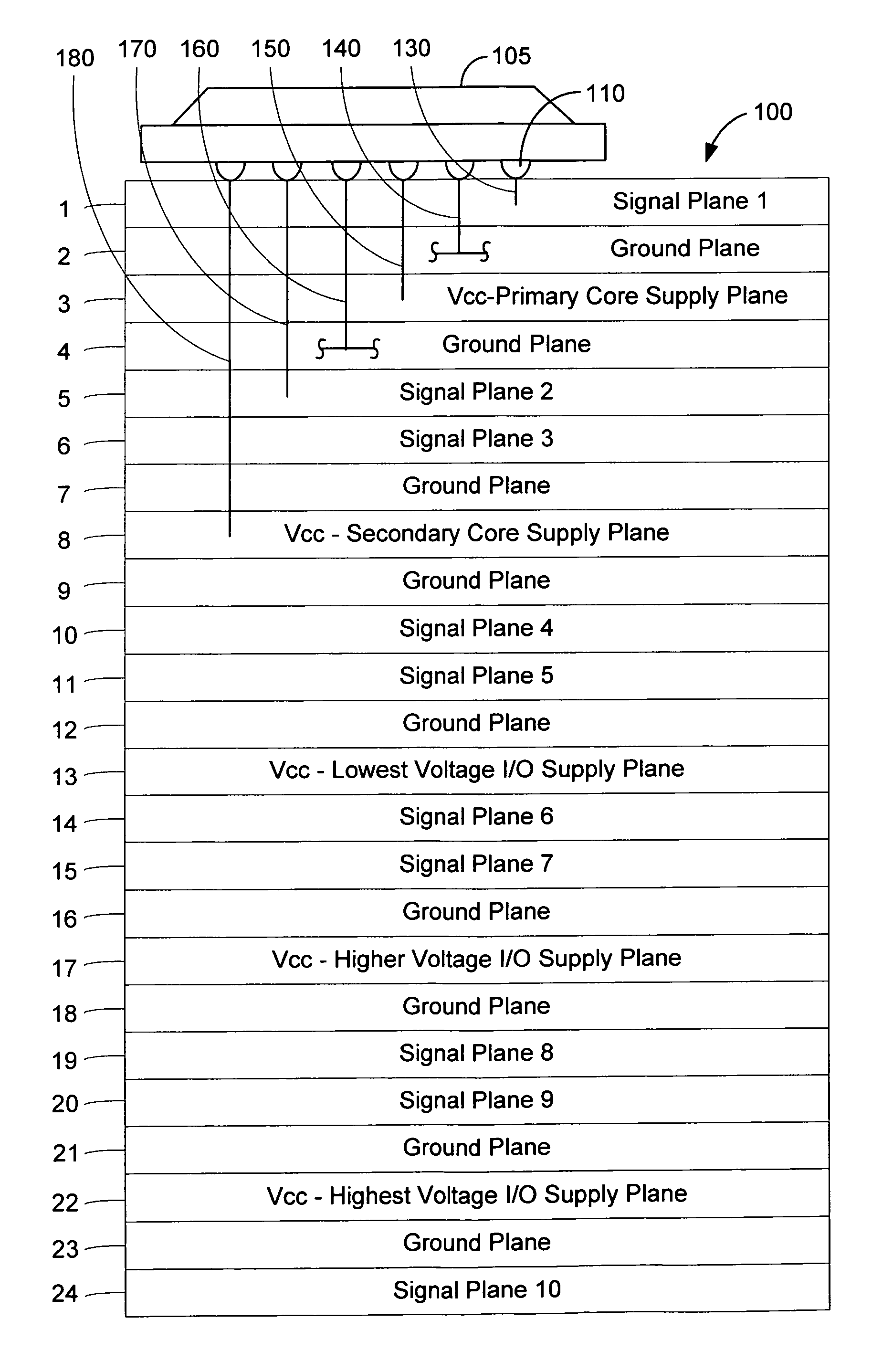
[0025]Various embodiments of the present invention provide for reducing the amount of jitter on a clock as it propagates through a PCB to and through a silicon device, such as a FPGA. Jitter can be suppressed by minimizing the amount of ripple, both peak-to-peak amplitude and oscillation, present on the internal voltage rails that drive timing-critical circuitry on the FPGA. These voltage rails run through planes of the PCB to and through the FPGA. Examples of a FPGA's timing-critical circuitry are clock trees, delay lines, and digital clock management (DCM). These circuits operate on the primary core voltage. A clock tree distributes the system clock signal from a common point to all the elements of the system using the clock signal. A delay line is a transmission line or equivalent device, such as an analog delay line, used to delay a propagating signal. A delay line as described herein can also include a physical device such as a buffer used to provide a controlled delay between ...


PUM


Abstract

A model and method are provided for lowering device jitter by controlling the stackup of PCB planes so as to minimize inductance between a FPGA and PCB voltage planes for critical core voltages within the FPGA. Furthermore, a model and method are provided for lowering jitter by controlling the stackup of package substrate planes so as to minimize inductance between a die and substrate voltage planes for critical core voltages within the die.

Description

BACKGROUND[0001]1. Technical Field[0002]The present invention relates to printed circuit boards (PCBs) and package substrates, and more particularly to the reduction of jitter in a semiconductor device by controlling stackup.[0003]2. Related Art[0004]Programmable logic devices (PLDs) are a well-known type of integrated circuit (IC) that may be programmed by a user to perform specified logic functions. One type of PLD, the field programmable gate array (FPGA), typically includes an array of programmable tiles. These programmable tiles can include, for example, programmable input / output blocks (IOBs), configurable logic blocks (CLBs), dedicated random access memory blocks (BRAMs), multipliers, digital signal processing blocks (DSPs), processors, clock managers, delay lock loops (DLLs), and so forth. Notably, as used herein, “include” and “including” mean including without limitation.[0005]One such FPGA is the Xilinx Virtex® FPGA available from Xilinx, Inc. of San Jose, Calif. 95124. A...

Claims


Application Information

Patent Timeline
Patent Type & Authority Patents(United States)
IPC IPC(8): H05K1/00
CPCH05K1/0216H05K1/0262H05K1/0298H01L2924/15311H05K2201/10212H05K2201/10734H01L2224/16H05K2201/09327
Inventor DUONG, ANTHONY T.
Owner XILINX INC
Why Eureka
Try Eureka