Method and apparatus for low inductive design pattern

a low inductance, design pattern technology, applied in the direction of cross-talk/noise/interference reduction, printed capacitor incorporation, printed electric component incorporation, etc., to achieve the effect of minimizing the inductance of the packaging substra

Inactive Publication Date: 2012-07-12
ALTERA CORP
View PDF4 Cites 2 Cited by
  • Summary
  • Abstract
  • Description
  • Claims
  • Application Information

AI Technical Summary

Benefits of technology

[0004]Broadly speaking, the present invention fills these needs by providing a spatial arrangement that minimizes inductance for the packaging substrate. It should be appreciated that the present invention can be implemented in numerous ways, including as a method, a system, or an apparatus. Several inventive embodiments of the present invention are described below.
[0005]In one aspect of the invention, an interleaved or wavy spatial arrangement of the micro-vias providing the electrical pathways for the power and ground leads are described. The spatial arrangement increases the coupling pairs between power and ground vias or leads. This spatial arrangement is maintained even as the micro-vias transition across a plane from a direction of travel. That is, since the micro-vias cannot be stacked vertically on the same axis the entire width of the packaging substrate due to manufacturing constraints, the axis of travel through the substrate transitions within a conductive plane. Even with this transition, the interleaved or wavy spatial arrangement is maintained. Thus, the charge from the decoupling capacitor is able to more efficiently be delivered as the inductances are minimized through this design.

Problems solved by technology

That is, since the micro-vias cannot be stacked vertically on the same axis the entire width of the packaging substrate due to manufacturing constraints, the axis of travel through the substrate transitions within a conductive plane.

Method used


Image

  • Method and apparatus for low inductive design pattern
  • Method and apparatus for low inductive design pattern
  • Method and apparatus for low inductive design pattern

Examples


Embodiment Construction

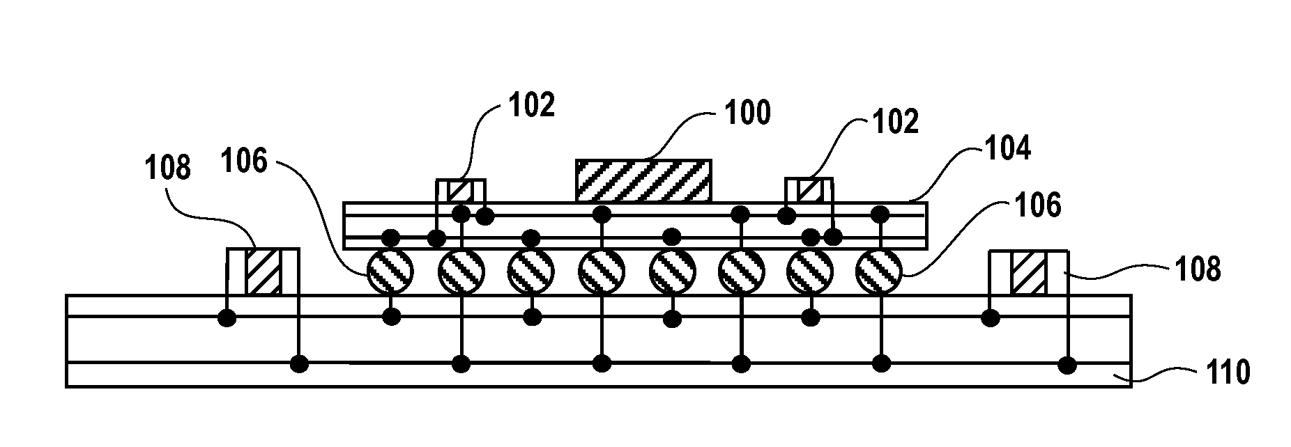
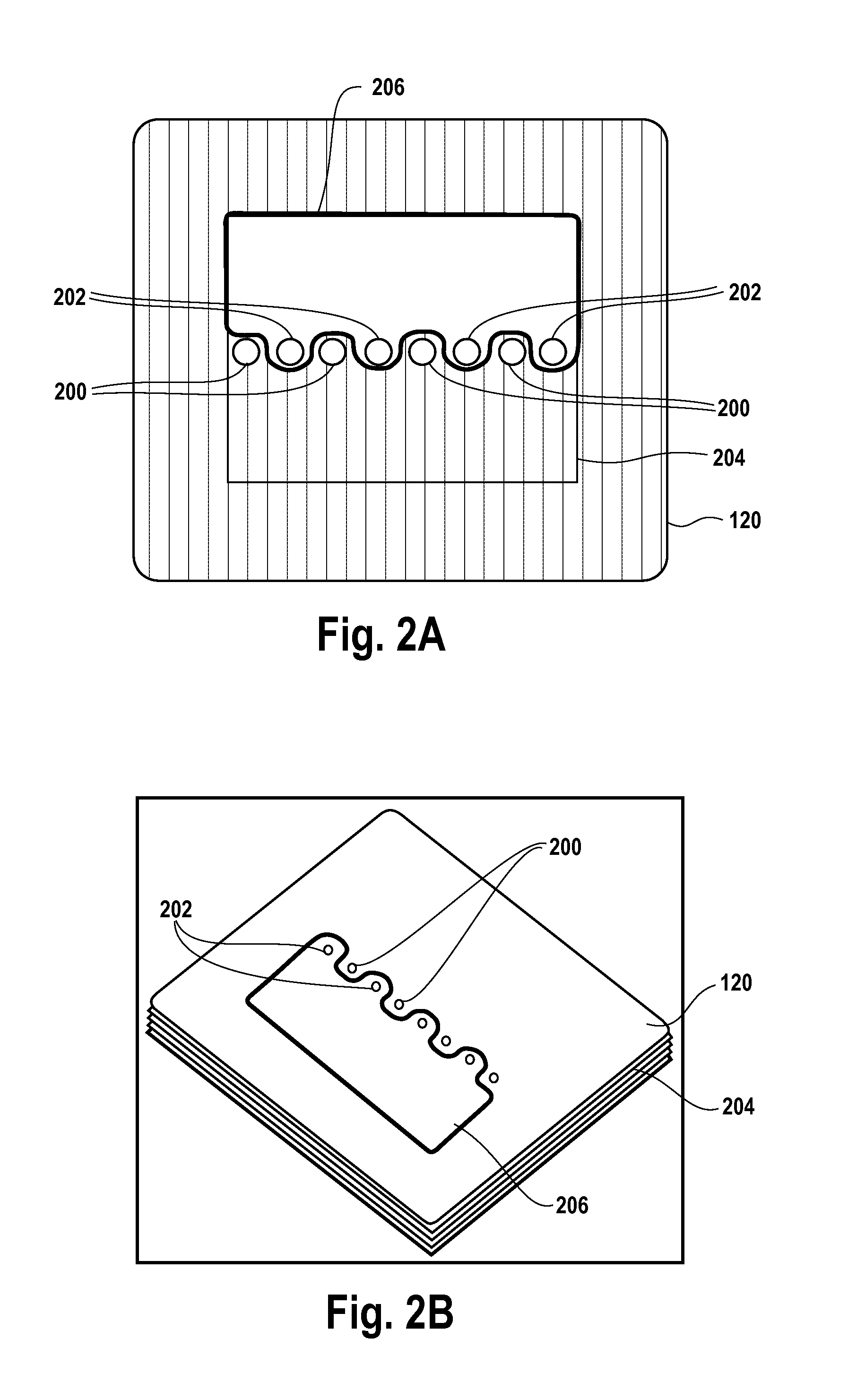
[0014]The embodiments described herein discuss interleaving power and ground planes so that micro via patterns can be interleaved accordingly in order to enable the charge released by the capacitor to reach the device quickly and effectively. It will be obvious, however, to one skilled in the art, that the present invention may be practiced without some or all of these specific details. In other instances, well known process operations have not been described in detail in order not to unnecessarily obscure the present invention.

[0015]The embodiments described herein provide for interleaving micro-vias within a package substrate in order for a charge to reach the device more quickly. This interleaving increases the coupling between the power and ground vias so as to increase the coupling pairs of the power and ground vias. The interleaving, or disposing of adjacent pairs between each other as described below, enables a reduction in the inductance therebetween. Thus, through the embod...


PUM


Abstract

Provided is an interleaved or wavy spatial arrangement of the micro-vias providing the electrical pathways for the power and ground leads are described. The spatial arrangement increases the coupling pairs between power and ground vias or leads. This spatial arrangement is maintained even as the micro-vias transition across a plane from a direction of travel. Thus, the charge from the decoupling capacitor is able to more efficiently be delivered as the inductances are minimized through this design.

Description

PRIORITY[0001]This application is a divisional application of U.S. application Ser. No. 12 / 034,353, filed Feb. 20, 2008. The disclosure of this related application is incorporated herein by reference for all purposes.BACKGROUND[0002]Packaging configurations for semiconductor circuits typically include mounting of the die having the integrated circuit to a substrate, which in turn is mounted onto a printed circuit board or another substrate. Decoupling capacitors provide a momentary charge to compensate when active devices change current consumption. This momentarily stabilizes the current fluctuation caused by the changing current consumption of the integrated circuit, thereby attenuating impedance fluctuations caused by the varying current consumption. The charge in the decoupling capacitors is replenished from the power supply that is connected between each power plane and ground. As packaging substrates are becoming more complex due to the increasing complexity and the miniaturiz...

Claims


Application Information

Patent Timeline
Patent Type & Authority Applications(United States)
IPC IPC(8): H01L21/50
CPCH01L23/49822H01L23/49838H01L23/50H05K1/0224H05K1/0231H05K1/162H05K2201/093H01L2924/0002H05K2201/097H05K2201/0979H01L2924/15311H01L2924/19105H01L2924/00
Inventor CHANG, LI-TIEN
Owner ALTERA CORP
Why Eureka
Try Eureka