Power semiconductor module and power semiconductor circuit configuration

a technology of power semiconductor modules and circuit configurations, which is applied in the direction of solid-state devices, electric devices, transportation and packaging, etc., can solve the problems of synchronous triggering of power semiconductor modules connected in parallel, the development of power semiconductor modules is particularly difficult, and the time difference between switching individual semiconductor chips is increasing. , to achieve the effect of preventing an overload of individual diodes, and reducing the generation of inductan

Inactive Publication Date: 2012-09-06
ROBERT BOSCH GMBH
View PDF7 Cites 0 Cited by
  • Summary
  • Abstract
  • Description
  • Claims
  • Application Information

AI Technical Summary

Benefits of technology

[0014]An improved symmetry of the linkage of the individual power switch chips to the intermediate circuit using at least one intermediate circuit capacitor is achieved by dividing at least one of these terminals into at least two partial terminals. In the ideal case, the voltage offset at the emitter or source terminals of the power switches which is important for symmetrical triggering of the power switches and is caused by rapid current changes during a commutation operation may be eliminated completely by such a configuration. Therefore, in comparison with power semiconductor modules such as those known in the related art, the synchronicity of the triggering and thus of the utilization of the chip area of the individual power switches is easily increased substantially.
[0015]In addition, a homogeneous current transfer of parallel connected diodes during the cut-off of the power switches is also ensured due to decoupling of the individual commutation circuits, thereby preventing an overload of individual diodes.
[0016]According to one specific embodiment of the present invention, an intermediate circuit terminal having a positive supply voltage potential and an intermediate circuit terminal having a negative supply voltage potential are situated in direct proximity to one another on the substrate. The intermediate circuit terminals are situated as close to one another as possible, to thereby minimize the inductance generated by the terminal pairs. The dielectric strength is the limiting factor, which may also be increased further by using an insulation film between the two terminals.
[0018]According to one advantageous specific embodiment of the power semiconductor circuit configuration, an intermediate circuit terminal having a positive potential and an intermediate circuit terminal having a negative potential are each situated directly adjacent to one another on the power semiconductor module, and the feeder lines connected to them are carried preferably in parallel up to the intermediate circuit capacitor. The inductance generated by the feeder lines may also be reduced in this way.

Problems solved by technology

However, at switching frequencies of more than 1 kHz in particular, synchronous triggering of power semiconductor modules connected in parallel is difficult because the contact resistances of the control lines may vary greatly under some circumstances, in particular with an increase in lifetime, which results in a progressive increase in the time difference during switching of the individual semiconductor chips.
However, particular challenges arise in the development of power semiconductor modules having multiple power switches connected in parallel within a module.
Overvoltage spikes are induced on the power switches due to inductances in the commutation circuit.
Since the maximum blocking voltage of the individual power switches is limited, excessive overvoltages result in destruction of the power switches.
The result is an uneven distribution of load among the power switches, which may thus result in an overload of individual power switches and ultimately in a shortening of the lifetime of the power semiconductor module.
Finally, an asymmetrical electrical configuration of the diodes may result in the current not being divided evenly among the diodes immediately after cut-off of the power switches, which may cause an overload of individual diodes.
This problem is further exacerbated by power diodes having a negative temperature coefficient below approximately 75° C., which means that at low temperatures, a diode which is under a greater load anyway due to the switching will carry an increased current, also in steady-state operation, in comparison with the other diodes connected in parallel.
Ultimately an asymmetrical electrical configuration of the diodes may also shorten the lifetime of the power semiconductor module.
Since an increase in the blocking voltage results in greater losses in the power switch chip due to the technology used and thus the required chip area increases for the same inverter specification, usually an attempt is made to reduce the inductance in the commutation circuit.

Method used


Image

  • Power semiconductor module and power semiconductor circuit configuration
  • Power semiconductor module and power semiconductor circuit configuration
  • Power semiconductor module and power semiconductor circuit configuration

Examples


Embodiment Construction

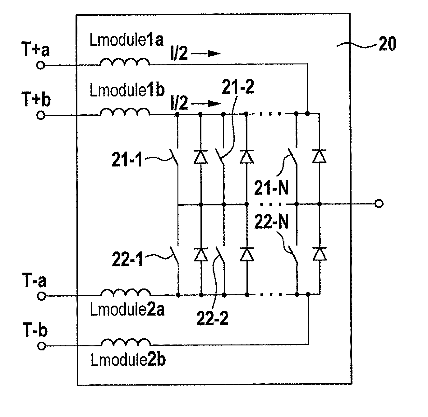
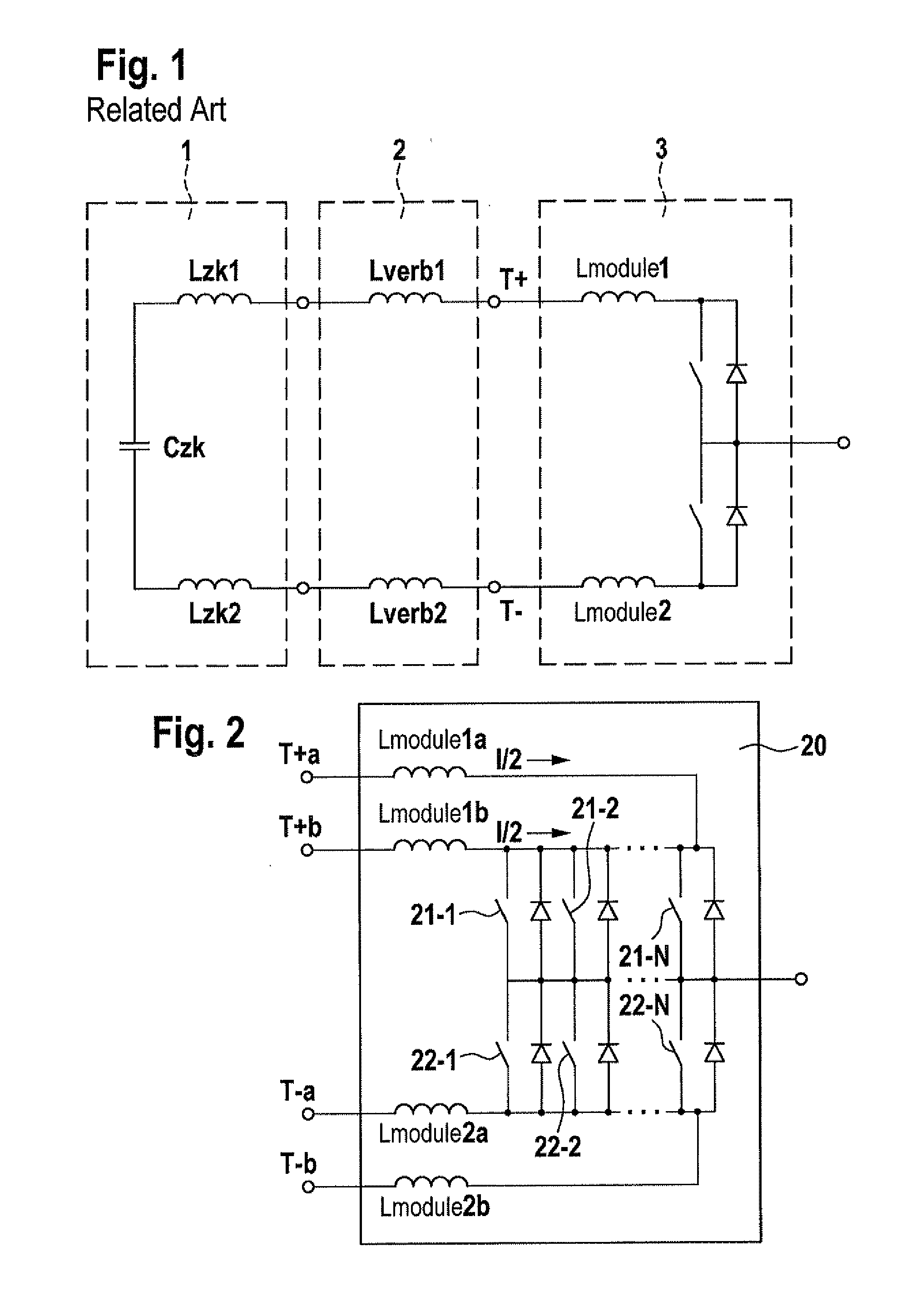
[0026]FIG. 2 shows a simplified equivalent circuit diagram of a power semiconductor module 20 according to the present invention for use in an inverter. Power semiconductor module 20 includes a parallel circuit of N circuit paths, each having a series connection of a high-side power switch 21-1 through 21-N and a low-side power switch 22-1 through 22-N, one diode being connected in parallel to each power switch 21 and 22. The terminals of high-side power switches 21 facing away from low-side switches 22 are each connected to a positive supply voltage potential. Two intermediate circuit terminals T+a and T+b are provided, one of the terminals, namely terminal T+b in the example shown here, advantageously being contacted in the area of a first exterior circuit path, namely the left exterior circuit path in this example, whereas the second terminal, namely terminal T+a in the example shown here, is advantageously contacted in the area of the external circuit path situated at a distance...


PUM


Abstract

A power semiconductor module having a substrate, at least two power semiconductor switches being situated on the substrate and connected in parallel, at least one intermediate circuit terminal for connecting the power semiconductor switches to a first supply voltage potential and at least two intermediate circuit terminals for connecting the power semiconductor switches to a second supply voltage potential, one of the supply voltage potentials being negative and the other being positive.

Description

FIELD OF THE INVENTION[0001]The present invention relates to a power semiconductor module and a power semiconductor circuit configuration.BACKGROUND INFORMATION[0002]Polyphase machines, which are operated in combination with inverters—frequently also referred to as power inverters—are used for the drive in hybrid or electric vehicles. An inverter includes at least one power semiconductor module having semiconductor components in the form of power semiconductor switches—hereinafter referred to simply as power switches—for example, MOSFETs (metal oxide semiconductor field-effect transistors), IGBTs (insulated gate bipolar transistors) or MCTs (MOS-controlled thyristors), usually in combination with free-wheeling diodes. Through suitable internal wiring within the module, different circuit variants, such as individual switches, half bridges, whole bridges or also choppers, may be implemented. The individual power switches are usually designed in the form of semiconductor chips situated...

Claims


Application Information

Patent Timeline
Patent Type & Authority Applications(United States)
IPC IPC(8): H02M7/537
CPCB60L3/003B60L3/0092H01L25/072H02M7/537H01L2924/0002H02M1/32H01L2924/00
Inventor SCHOENKNECHT, ANDREAS
Owner ROBERT BOSCH GMBH
Why Eureka
Try Eureka