Methods of fabricating nanoscale-to-microscale structures

a technology of micro-scale structures and nano-scales, which is applied in the field of three-dimensional nano-to-micro-scale structures, can solve the problems of large untapped potential for the use of new three-dimensional nano-to-, micro-scale devices, and the difficulty of developing processing protocols that meet both of these often-conflicting requirements of scalability and precision, and achieves attractive electronic or optical properties, high strength, and high scalability.

Inactive Publication Date: 2009-11-10
GEORGIA TECH RES CORP
View PDF5 Cites 61 Cited by
  • Summary
  • Abstract
  • Description
  • Claims
  • Application Information

AI Technical Summary

Benefits of technology

[0039]The present invention particularly provides attractive means of producing freestanding nanostructured micro-assemblies of silicon, silicon solid solutions, silicides, silicon carbide, or silicon nitride for use in electronic, optical, chemical, or mechanical applications. Nanostructured silicon-based devices can exhibit attractive electronic or optical properties (e.g., photoluminescence). Nanostructured silicon carbide-based devices and silicon nitride-based devices can exhibit attractive electronic, chemical, and / or mechanical properties (e.g., high strength).

Problems solved by technology

However, a far larger untapped potential exists for the use of new three-dimensional nanoscale-to-microscale devices in a variety of advanced applications, such as in:
Developing processing protocols that satisfy both of these often-conflicting requirements of scalability and precision remains a significant challenge.
Such limited chemistries severely restrict the properties (e.g., electronic, biomedical, chemical / catalytic, optical, thermal) of such micro / nanostructures for device applications.
Work to date has not demonstrated, however, how nanostructured micro-assemblies (such as diatom microshells) may be reactively converted into inorganic replicas comprised solely of an element (such as silicon), a metallic alloy (such as a silicon alloy), or a non-oxide compound (such as silicon carbide or silicon nitride).

Method used


Image

  • Methods of fabricating nanoscale-to-microscale structures
  • Methods of fabricating nanoscale-to-microscale structures
  • Methods of fabricating nanoscale-to-microscale structures

Examples


examples

Conversion of Diatom Microshells into Silicon Replicas

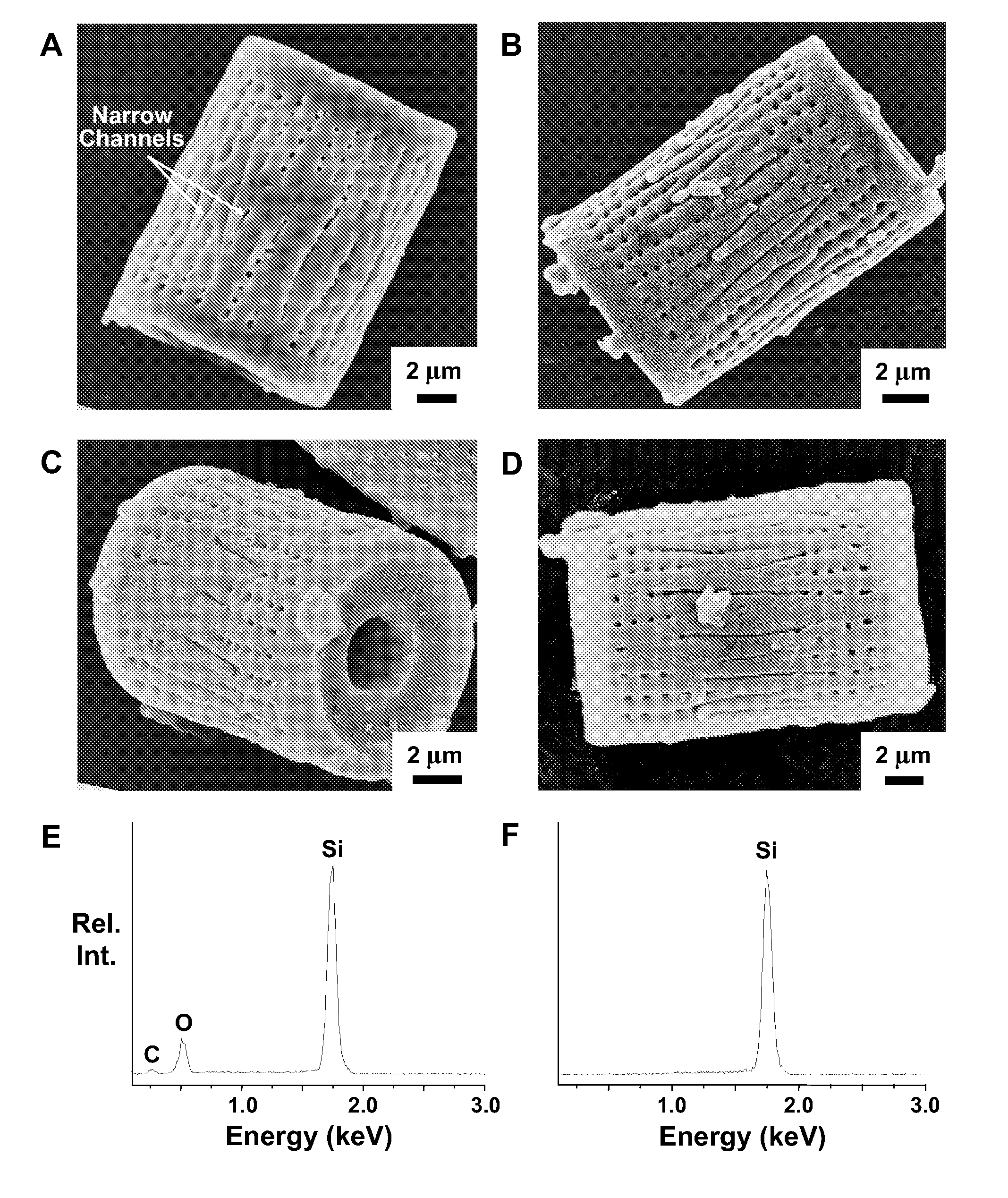
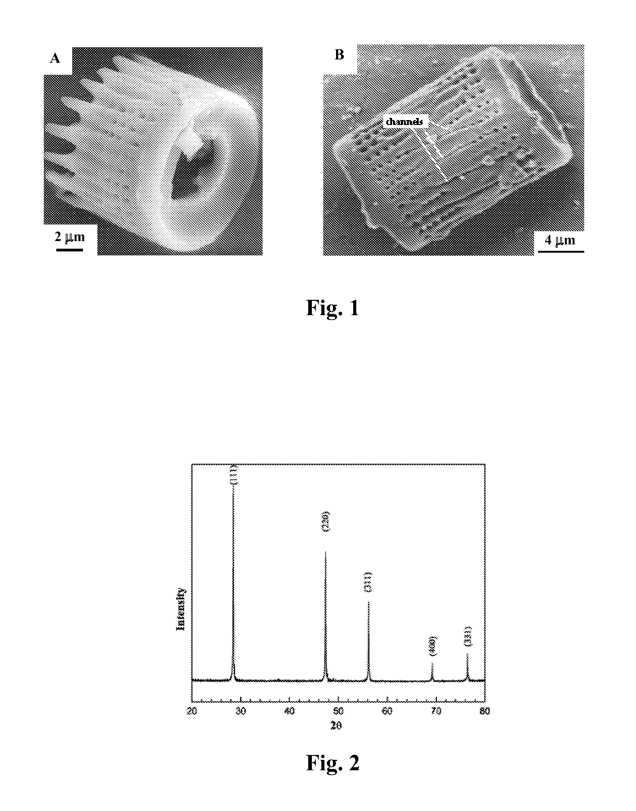
[0106]Cylindrical SiO2-based Aulacoseira diatom microshells were utilized as three-dimensional nanostructured microtemplates. Secondary electron images of the starting Aulacoseira diatom microshells are shown in FIG. 1. Half of an Aulacoseira microshell is shown in FIG. 1A, and a complete microshell is shown in FIG. 1B. The exposed end of the half microshell in FIG. 1A possesses a circular hole and a protruding rim. The other end contains fingerlike extensions and is closed. Rows of fine pores running parallel to the length of the cylindrical microshells can be seen in both FIGS. 1A and 1B.

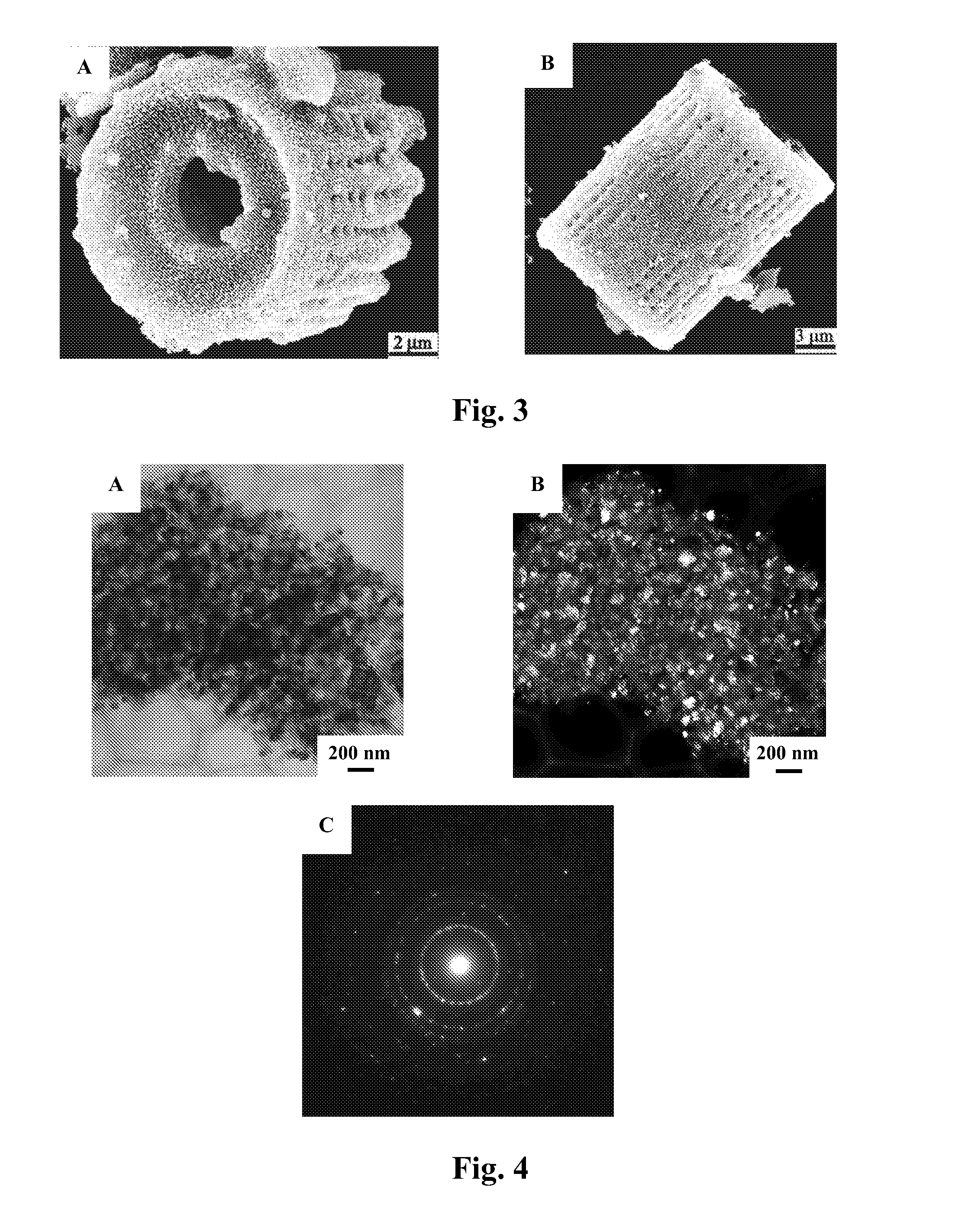
[0107]The Aulacoseira diatom microshells were sealed along with solid magnesium within a steel tube. The microshells and magnesium within the sealed steel tube were then heated to 900° C. for 1.5 hours to allow for evaporation of the magnesium and reactive conversion of the diatom microshells into replicas, comprised of MgO and Si, via the oxid...


PUM

PropertyMeasurementUnit
sizeaaaaaaaaaa
temperatureaaaaaaaaaa

Abstract

Methods for the production of shaped nanoscale-to-microscale structures, wherein a nanoscale-to-microscale template is provided having an original chemical composition and an original shape, and the nanoscale-to-microscale template subjected to a chemical reaction, so as to partially or completely convert the nanoscale-to-microscale template into the shaped nanoscale-to-microscale structure having a chemical composition different than the original chemical composition and having substantially the same shape as the original shape, being a scaled version of the original shape. The shaped nanoscale-to-microscale structure formed comprises an element (such as silicon), a metallic alloy (such as a silicon alloy), or a non-oxide compound (such as silicon carbide or silicon nitride).

Description

CROSS REFERENCE TO RELATED APPLICATION[0001]This application claims priority of U.S. Provisional Patent Application No. 60 / 837,465, filed 11 Aug. 2006, the entire content of which is hereby incorporated by reference.BACKGROUND OF THE INVENTION[0002]1. Field of the Invention[0003]The present invention relates generally to shaped three-dimensional nanoscale-to-microscale structures, and more specifically to methods of producing shaped nanoscale-to-microscale structures from nanoscale-to-microscale templates having an original chemical composition and an original shape, and subjecting the nanoscale-to-microscale templates to a chemical reaction, so as to partially or completely convert the nanoscale-to-microscale template into the shaped nanoscale-to-microscale structure having a chemical composition different than the original chemical composition and having substantially the same shape as the original shape, being a scaled version of the original shape.[0004]2. Description of Related...

Claims


Application Information

Patent Timeline
Patent Type & Authority Patents(United States)
IPC IPC(8): C01B13/14
CPCB81C99/0095Y10T428/256Y10T428/24479Y10T428/2998B33Y80/00Y10T428/31551Y10T428/31663
Inventor SANDHAGE, KENNETH HENRYBAO, ZHIHAO
Owner GEORGIA TECH RES CORP
Why Eureka
Try Eureka